Is it possible to dictate which side of the through hole gets the copper pad on a double sided board?
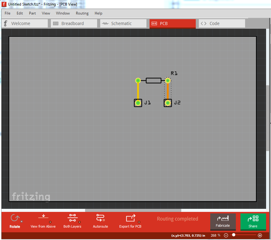
Welcome aboard! By default through hole parts have pads on both top and bottom layer. You can right click on a trace that connects to the pad and in the menu select move to bottom layer (or move to top layer if it is already on the bottom) to change which side of the board the trace is on. Here I have connected a resistor to 2 .1 in headers the trace on the left is on the top of the board and the trace on the right is on the bottom of the board (and is selected, if you right click on it, it will have a move to top of board option.)
Peter
Thanks,
So when i have this
I still get the pads showing up in the top side etch file where it shouldn’t be
The pads should be showing up on the top side, the assumption is that the holes are plated through so the top pad is connected to the bottom pad. What you need to do here is click on a trace and in Inspector (the lower right window) reduce the trace size from the default 24mils so it will go between the pads like this:
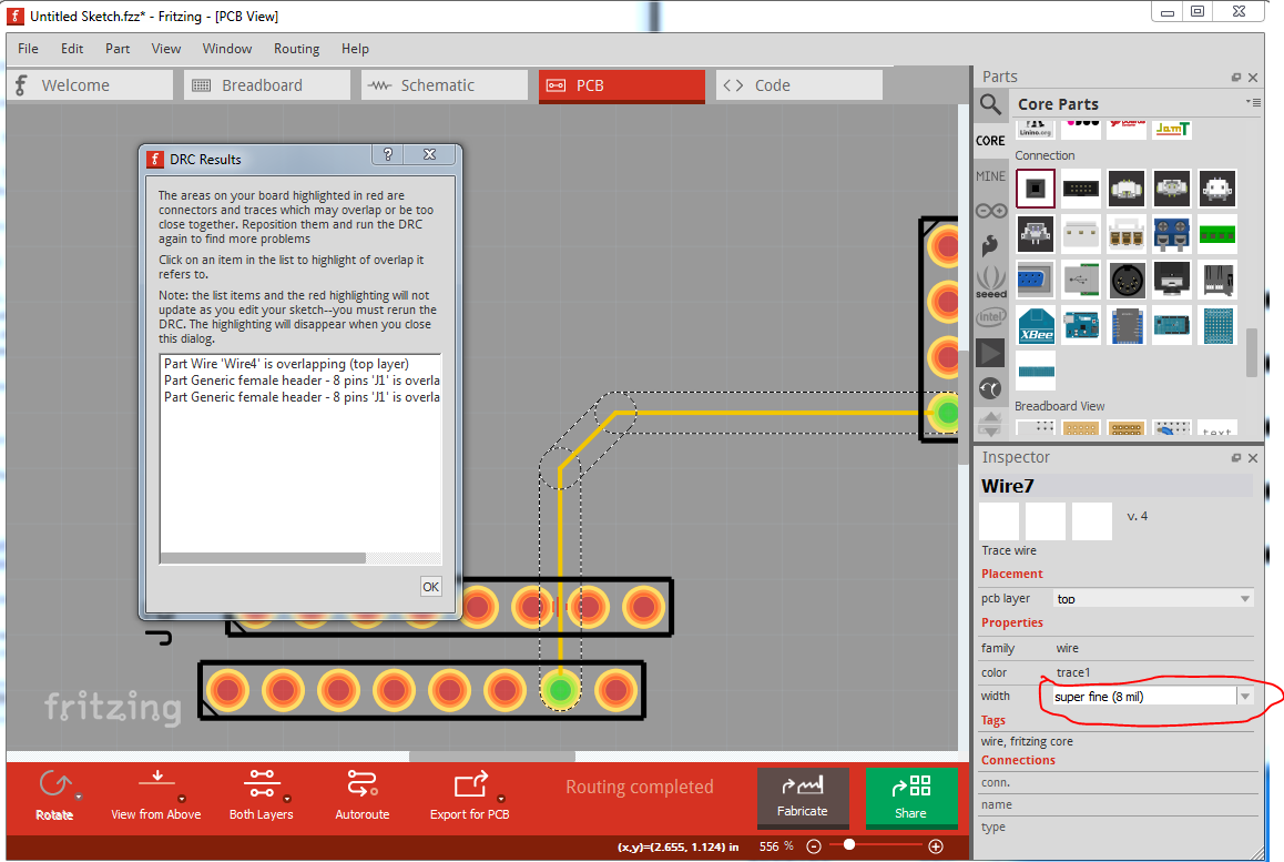
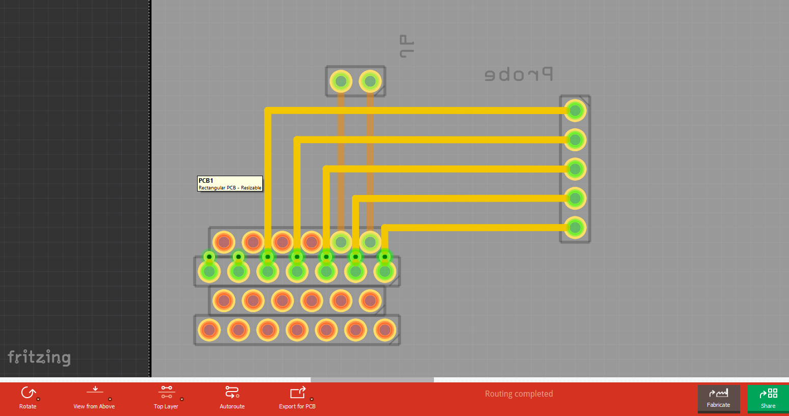
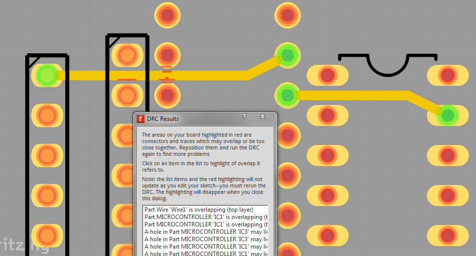
although as we see DRC (Routing-> Design rules check) is complaining that their is over lap but in practice a board house will accept and produce this without issue (I doubt it will work for home etch though.) That you really want (but Fritzing doesn’t at present have other than as custom parts) is something like this that I did for the Raspberry Pi 4B:
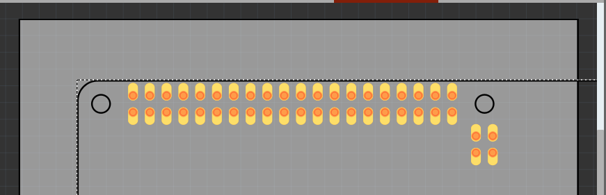
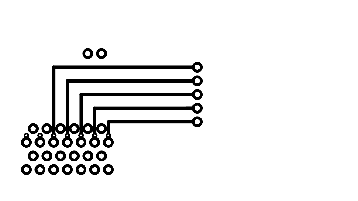
which has much more room between the pads to route traces. You also don’t need the vias on the traces, the pads connect through to the bottom layer if the board is plated through (or you solder a wire on both sides for home etched boards without plating through.) Here is the gerber output (displayed by gerbv) for the above board:
The pads are all on both layers but the trace is only on the top (orange.)
Peter
I’ll probably need to change it in a photo editor, as this is for in home etching. I’ll make the appropriate changes so that it can be made a board house for later,
I really appreciate explanation and help!
If you need only a few sizes (such as 6 positions and 7 positions in the example above) I can make custom parts easily enough that may be able to support home etching (you can get up to 12mil traces between the pins of the RPI 4B connector without DRC complaining.) To make the parts factory generate this pattern requires a code change that isn’t done yet, although it is planned, and that in turn means a new release which is somewhere in the future.
edit:
OK here are a 6 pin and 7 pin header test parts which will implement your example (if you need other sizes they are easy to produce.) I’d suggest trying really hard to keep all the connections to the headers on the bottom layer for easy soldering (without plated through holes it will be hard to solder the top of a header!) With 16mil traces it passed DRC so I think it should probably work on home etch. I learned I needed to shorten the oblong pads to allow for .1 in spaced connectors without shorting.
test sketch:
teast-sketch.fzz (14.7 KB)
parts:
oblong-male-header-6-pins.fzpz (5.0 KB)
oblong-male-header-7-pins.fzpz (5.1 KB)
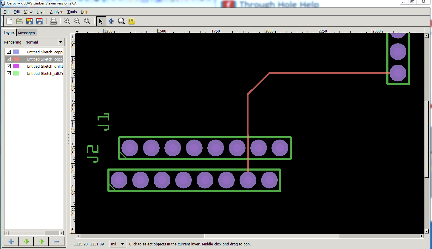
and the gerber output from the test sketch:
note I didn’t obey my advise and routed traces on both sides to make sure I could … Also these are male pins, if you need female that is a trivial change as well. As you look to have already discovered, the grid size here is 0.05in (rather than the default 0.1in) to allow the traces to route between the .1 pins. Hope this helps.
Peter
1 Like
These oblong pads are very useful, hope there was a option in generic IC pins.
Here one of atmega8 has it…
I think I should make some header pin parts using it…
You didn’t leave the hole empty, maybe it’s ok with gerber file, but in the home etching file those holes remain black… 
Also, the atmega8 pass the DRC check with 24mil trace… 
I had started modifying the parts factory code to fix a bunch of things (incorrect scales, overly complex svg, too long pins) before getting distracted by trying to restart development. When I get back to it, I intend to fix double sided headers in breadboard (they are currently broken), add options for 2mm , 1.27mm and 1mm headers (with the correct pads sizes, as you can do 2mm now if you adjust the pad size in Inspector) and a choice of oblong pads for all of headers, the generic ICs and the mystery part. I know where the code is and how to do it (which is unusual for me in the Fritzing sources ![]() ) it’s just a matter of getting back to it. FritzingCheckPart.py improvements first though and that is going slow!
) it’s just a matter of getting back to it. FritzingCheckPart.py improvements first though and that is going slow!
The difference is IC pins have a 0.035in (or maybe 0.030) hole and header pins have 0.038in the 3 thou extra makes all the difference, although I’ll look at trimming the surround down a bit (from stroke-width 10 to stroke-width 5 may do it.) But I think that may make the edge of pad by the hole too thin. I think minimum feature size for the inexpensive board houses is about 8 thou and that would be 5 thou. Being able to pass DRC with a 24mil trace is desirable however especially for something in parts factory.
edit: they split the difference, the hole is 0.032in, but I’ll still try a stroke-width 0f 5 and see what happens.
edit1:
My network connection has been down most of the day but I did manage to get something that passes DRC with the standard 24 mil traces by reducing the size of the pads by a bit. I think the OP may want to use the bigger pads above, but he could try these if he is feeling adventurous ![]()
edit2:
I have fixed these two (by changing the path and circle) so they generate the hole in the export as pdf which they were not doing (thanks to @Blue for the heads up!) If you have downloaded them, please download the new ones below.
oblong-male-header-6-pins.fzpz (5.0 KB)
oblong-male-header-7-pins.fzpz (5.2 KB)
edit3:
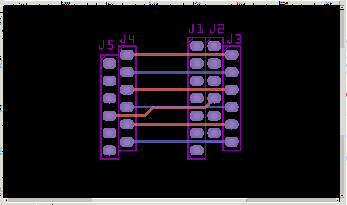
I just ordered some boards with this layout (which is an rs232 breakout board, an IDC DB9 on each end for the serial connection and a monitor port in the middle.)
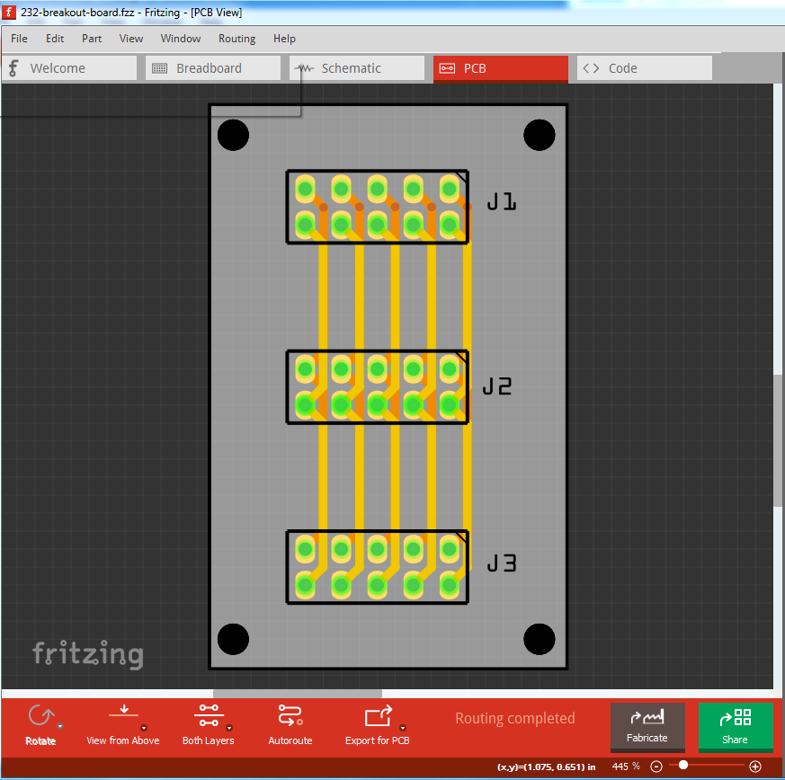
232-breakout-board.fzz (25.8 KB)
as a test of the new footprint before modifying the parts factory to use it as an option.
Peter