https://images.app.goo.gl/SBVQhyYgviyd4Dor6
@microMerlin Here you can find the dimensions.
Yup, a PCB would be fine for this one… 
https://images.app.goo.gl/SBVQhyYgviyd4Dor6
@microMerlin Here you can find the dimensions.
Yup, a PCB would be fine for this one…
Worse than that, this is going to need a very odd pcb layout specifically this one:
which is not a beginner type project. I’ll have a look at making one of I can get a copy of the jpg spec file somehow.
Peter
That last link posted is not a proper datasheet, but it does look like enough dimension information to do a footprint from.
From earlier reading, I did not think the PCB SVG would be that complex to create (manually). It should Just need the copper0 layer after copper1, instead of inside. There are no duplicate connector pins to mess things up, which happens where there is a mix of THT and SMD connectors in a single part. This is all SMD connectors, just both sides.
If I was doing it, I would get one side set up like a normal SMD part, then copy / paste the single copper layer, change the name of the layer, change the pin numbers in the second layer. Done.
@microMerlin @vanepp
Give this connector a try. A one with PCB base with copper0 and copper1 layer may be fine. GoodLuck friends. 
Here is an almost part. It is almost because there is no specification for the spacing between rows on the connector, so this is just a guess based on the jpg image (and thus perhaps not accurate,) Either print out the pcb footprint and check the spacing before ordering boards or measure the space between the rows of pins (preferably with vernier calipers.) The pin pitch appears to be standard 0.156in (but check that too!)
Jamma-edge-connector.fzpz (11.8 KB)
I was thinking of the board that plugs in to this connector, indeed this connector is fairly easy to make (other than the noted lack of a row spacing.)
Peter
I was thinking of the board too, which (for pcb) is the fingers/pads (at the edge) that the connector attaches to. A footprint with 2 rows of pads, one top, one bottom, exactly on top of each other. Where row spacing does not apply. It is the thickness of the pcb, which is the “z” direction, and not something Fritzing (or Gerber) cares about.
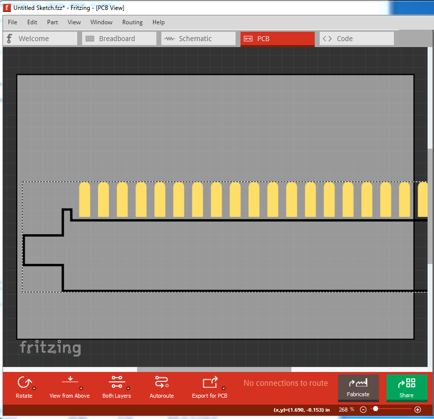
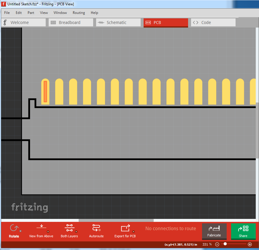
@vanepp Here is a sketch with a test version of your part using the pcb edge fingers. For discussion. Does it look like it should work? Would you do differently (other than getting rid of the translates I used)?
jamma-edge-test.fzz (15.6 KB)
I had to do more than expected to get the traces to work correctly. I Think I could have done it by using a variation of the oblong through hole pads, where copper layer graphic elements without an id are used to extend the pads around the main connectorNpin elements. However, I thought it likely that would break due to a bug in the way Fritzing decides what non-labeled graphics to include in the same net. Supposedly fixed in 0.9.4, but I am not trusting 0.9.3 when the extended area is much larger than the connector pin graphics.
Instead, I used connectpin ids on path elements for the full area, and added (unusual in pcb) connectorterminal elements to get connected traces to end in a reasonable spot.
Top and bottom traces now seem to work well (only by displaying only one layer at a time), but I think I hit a different DRC bug. It is complaining the pads on opposite sides of the pcb are overlapping. Gerber output looks OK, so I think it is just DRC. Hovering over pins also always shows the top layer information, even when set to Bottom layer, with the view for top turned off.
I used 4mm spacing on the pins, instead of 3.96mm, since that is what the posted image link showed. This is missing some other measurements to be accurate. I included a silkscreen outline for the body of the part, even though it will be almost complete off of the pcb board, in an effort to show where the edge of the board should be. But the available measurements do not show either the proper relationship between the edge of the board, and the start of the copper fingers, or the length of the fingers. So this is proof of concept. FritzingCheckPart complains all over this. It sees the copper1, copper0 in the fzp, decides it is THT, then complains when there is no radius to create a hole in the pcb. For every pad and terminal. It also complains that copper0 should be inside of copper1 instead of after, though there is no overlap/duplication in the pads and terminals. This type of part is not something that was considered when FCP was being written. Parts editor would probably either choke on this, or mess it up badly. I do not think it has a way to set individual connectors as top or bottom.
This looks good! There is a bug in that the pcb pin highlighting doesn’t appear til you mouse over the pin:
moved the mouse over the first pin (didn’t need to click, just mouse over) and the connection marker appears.
but that is minor. I’ll edit the howto and add this as an easier alternative if you don’t need through hole connections in the part. I expect most of the time you can make the part with no through holes and use vias in the sketch to getthe bottom pins to the other side of the board which will make life easier. Good thought!
Peter