The fzp part definition file has a bunch of empty bus entries.
The taxonomy entry says “part.dip.100.pins”. This is not a dip.
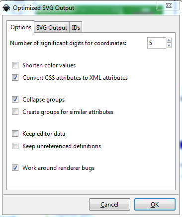
When I try to save the breadboard as optimized svg, Inkscape (actually output_scour.py) crashes on the save. Something about an element not in a list. It works on other files.
the schematic view does not need 8 copies of GND, or multiples ov VCC/VDD pins. The bus entries will handle that.
the schematic is using 0.2 inch long pins, instead of 0.1.
there seem to be some header blocks (graphics) on the breadboard that do not have connectors.
It is going to take some effort to really clean this up.
I don’t know XML - same as a beginner would - so I don’t know what half of that is.
FZ it’self tells you to make parts from other parts, so I made it out of a 100pin DIP.
The BB is a problem, but I can’t do anything about it because I don’t know how to draw something as complicated as a logo. I actually didn’t draw much in the BB view except rectangles, all the rest was copied and pasted from FZ outputs or svgs on the net.
I could stack all the GND pins on top of each other, and it’s probably more correct, but it makes it hard for a beginner to do.
The 0.1" pins in SCH is not what is being done in FZ, ie, that is an out of date stipulation. 0.1" works with small parts, but are wildly disproportionate with large SCH parts, ie, it just looks weird. FZ it’self uses 0.2" for ICs.
I’m not interested in making debug pins active.
If it’s junk I can just delete my tutorials, ie, INK is so bad at drawing, and FZ is so bad at interpreting INK, that it’s probably better I don’t help people use FZ.
None very serious. Most of them are about terminalId in breadboard in the fzp file but not breadboard svg which is likely a parts factory issue.
I expect this is an Inkscape bug. On Inkscape 0.9.4 using this as the output format, saving as optimized svg works:
it saves fine (but doesn’t collapse the groups) and the error message sounds like python looking for an element that isn’t in the list.
I used to be of the same opinion (still am somewhat ) but the problem in schematic with multiple pins all in the same group is that only one connection can be made to the entire group. The result of that is that sometimes a wire won’t connect because there is already a connection elsewhere in schematic, so Fritzing won’t make another. Unfortunately overlaying the pins fixes that (even though I don’t like it.) The converse is (as in the Atmega2560 IC in core parts) if you don’t bus the pins that you overlay then routing breaks because not all the pins get connected to (and this one affects pcb as well!)
I don’t know if this is correct or not. I think the parts factory code is old and wasn’t updated. It is true that generic IC uses 0.2in pins, but that doesn’t match the graphics standard document (which I think came later.) The practical reason that I at least favor 0.1in pins in schematic is that it makes the parts smaller and thus more will fit on one page, although I agree they look a little odd on larger parts, my view is that the space saving is worth it. I’m hoping to eventually fix up the parts factory to emit parts that match the graphics standards, but it is going to be complicated because there is already version dependent code in there (for compatibility with older Fritzing versions.)
I wouldn’t say it is junk, it looks to be serviceable as it stands. As far as I can see the buses are correct and the non debug pins all seem to be active so it should work fine. If someone wants the debug pins for something, they can add them later. The lack of logos (which are hard to make!) doesn’t affect the Fritzing functionality, nor do the missing terminalIds in breadboard, Fritzing defaults to using the center of the pin, which is correct in this case.
This is more a case of Inkscape aiming for its primary market (CSS compliance ) and Fritizng having a different goal (and/or not being CSS compliant because it doesn’t need CSS.) That is a lot of the purpose of FritzingCheckPart.py to adjust the xml that Inkscape produces to match what Fritzing is expecting (and/or will tolerate.)
XML has special rules for how it needs to be structured, but much of the content (descriptions, tags) is just text. The file itself is plain text. I am no good at ‘drawing’ either. I can do schematic and pcb, because this is much closer to cadd/drafting. It is based on known dimensions. For schematic pin size, probably true. Removing the duplicate pins would help with that, making the overall part a bit smaller. What the fritzing code uses is not what the current recommendations are. The recommendations and standards changes over time as more is learned. The code has not kept up.
That is a lot of debug pins. I though it might be things like ICSP.
Even if the part is not finished/optimized, it does not mean the tutorials are wrong. Tutorials are about learning techniques. Steps on the road to create and improve.
AFAIK, INK just can’t draw stuff that FZ will accept. I tried drawing an oval pad a number of different ways in INK, and nearly every time FZ distorted it in the gerber. The INK XML translation format is just not reliable in FZ, and even in the past FZ had trouble with Illustrator, so maybe FZ is more the problem because it’s too pedantic.
I wasted days before I was able to draw an oval in INK that worked in the Gerber export, but as soon as I duplicated it it went haywire again, like this :-
I suspect the logos in my BB are doing the same thing, but I can’t do much more than copy and paste them from the net. This probably explains why Van’s part doesn’t have logos
You guys are experts in XML and can fix it, but how is a beginner going to do it. And because it’s murder seeing something that looks correct in INK but doesn’t work in FZ, it causes a lot of problems.
PS - I noticed Van’s BB drawing is a bit longer than the actual board
This was an exercise in making a part with no coding, and simple pasting of drawing out of FZ, so it’s not going to have the nicety’s.
There are a number of bugs in gerber generation (and a number of fixes for them in 0.9.5 which hasn’t been released yet.) However I have in the past figured out how to do oblong pads. The ones in here should work and be duplicatable and movable in Ink
I expect your problems may be related to translates. The gerber code sometimes has trouble with translates. These ones have all translates removed and they work for me. As I think you know, you need a path for the oblong part and a circle with the correct hole size in the middle of the oblong to get the hole correctly (and to be able to change it easily.) The gerber code will only accept a path which is circular (and then the hole size is difficult to determine) so a circular pad is always the better bet as far as I am concerned. If you have the xml from some of the failed oblong pads, I’ll have a look at them and see if I can point out what went wrong.
an import (from a jpeg or pdf) and a convert object to path in Ink (although I often have trouble with that) or using the path editor (which I’m not very good at) should be able to create logos. As you note I usually have trouble with it and skip the logos …
Interesting, since I used the dimensions in the datasheet for the board (as I don’t have an actual board.) I expect silkscreen in pcb will be the same then.
I expect until we get some of the bugs fixed and make some progress on parts editor or its successor, that some coding and xml awareness is pretty much a necessity to make good parts. Fixing up all the parts in core parts so they are consistent and meet the graphics standards will be another good start but it will take a lot of work (as many of the core parts have various errors!)
Yep, looks like I mistyped the 97mm as 99 (because it is 99.0 in the svg, and it wouldn’t be exact if it was a scaling error.) I’m fixing the original part and swiping your logos on the way by . Since I didn’t do pcb in the original the error is less serious than it could be but still needs fixing.


 . Since I didn’t do pcb in the original the error is less serious than it could be but still needs fixing.