while the recommended hole size is 1.5mm the actual pin appears to be .9mm and it is possible that the current hole size is big enough that it fits in most cases. The current part hole size is 0.04in or 1.016mm so the pin should fit (although perhaps tightly!) The recommendation may be for automatic insertion equipment which likely needs more clearance.
The standard in Fritzing for ring size is 20 thou (so 0.508mm). Which makes a little bit larger ring which is likely better. In Inkscape the hole size is set by
hole-size = pad-diameter - (2 * stroke-width)
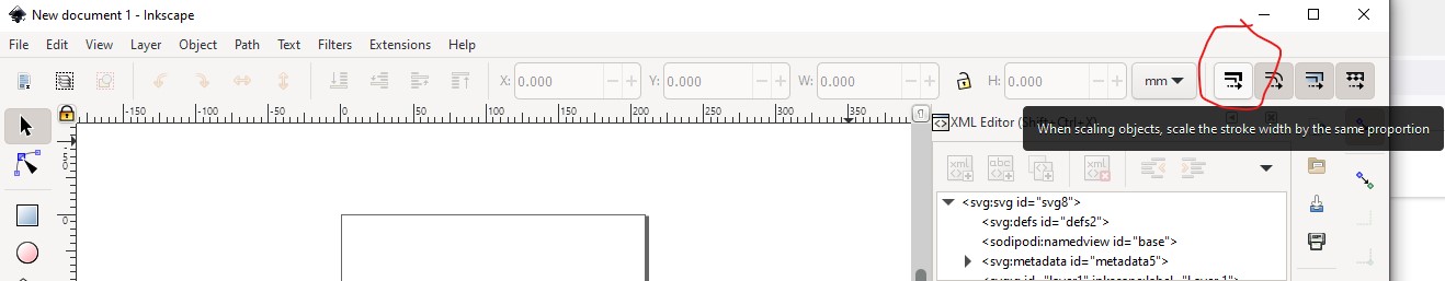
As to your problems with Inkscape changing sizes, there are two possibilities, one is if you have scale stroke width (the button circled in red in this image) which changes stroke-width when you increase the length of an element. I think it is on by default and I usually shut it off. That doesn’t entirely clear the problem though as stroke-width factors in to it in some circumstances. Then changing the coords multiple times to the values you want a couple of times converges on the values you want. You can also choose geometric mode in preferences, but it does something else undesirable that I don’t currently remember so I just live with it as is.
In your svg, connector1pin is attached to a group, which will work

but when you ungroup the connector name is lost. It is preferable to set it on the circle that is the connector as that won’t get changed in an ungroup. As well copper1 should be the first group (because it is the only group in a SMD part) with copper0 under it. I believe either way will work though.

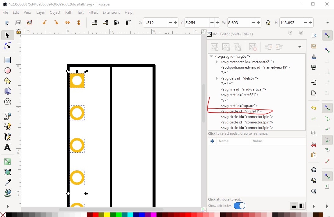
here I ungrouped the svg to rescale it and as we see connector0pin no longer exists.
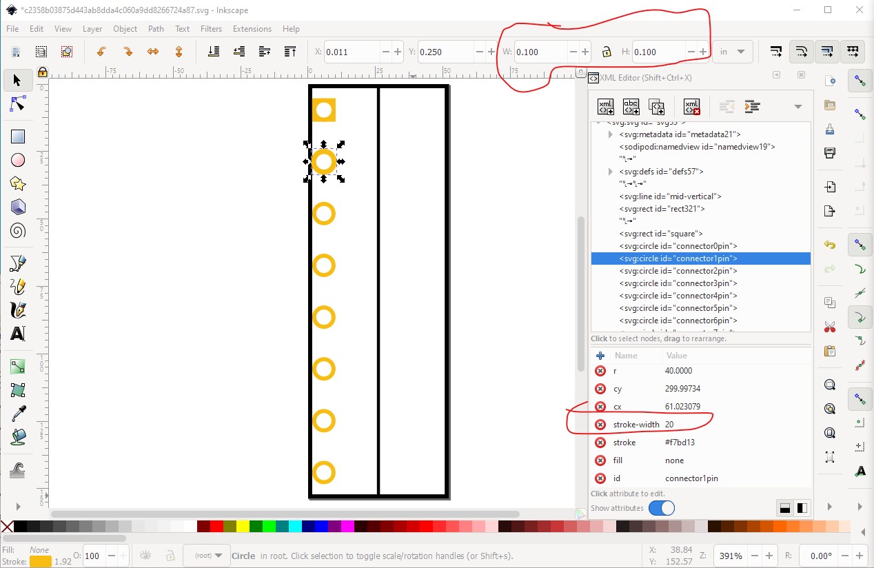
Here I rescaled the svg and set the stroke-width to 20 (20 thou) then changed the pad diameter to 0.1in giving a 0.06in hole which gets the ring size to the standard 20 thou. In Inkscape the way to do this is to change the pad diameters in the tool bar and note the new radius value in sml editor, then undo the two size changes to restore the old pad (because the size increase is from the left edge and top moving the center of the pad) and replace the radius with the new value (which increases the size of the pad from the center leaving it in the same place.)
Modifying the individual parts is indeed the only way to change this at present. There are a variety of suggestions for changes now that development is running again, but so far changing all the parts is it. It may need to remain it as the hole sizes in pcb are set from the pcb svg and changing that may be too difficult. we will have to see.
Peter