what units are the coordinates in pcb svg files in?
i’m trying to create a part for the camdenboss ctb0108-8 terminal block. i’m using fritzing’s built in ctb0158-8 as a starting point (the 015x series are 90 deg blocks, the 010x series are 0 deg; same pin spacing; datasheet for both). all i really want to do is edit the silkscreen outline.
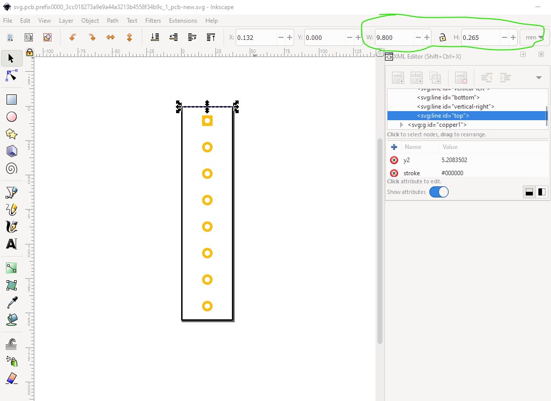
but i can’t make any sense of the units in the svg file. for example, here are 3 adjacent pins from fritzing’s svg (edited for brevity):
each of those is 14.4 units apart in y. this part has 5.08 mm pitch:
5.08 mm ≠ 14.4 so the svg isn’t mm
5.08 mm = 0.2 in ≠ 14.4 so the svg isn’t inches, 1/100 inches, or thou.
5.08 mm = 0.0167 ft ≠ 14.4 so the svg isn’t in feet
5.08 mm = 5.37 x 10⁻¹⁹ light years ≠ 14.4 so it isn’t light years
now i noticed that the speed of sound in nitrogen at 26.25 C and atmospheric pressure is roughly 352.8 m / s. i also noticed that 5.08 mm / (352.8 m / s) = 14.4 microseconds.
so as far as i can tell – and please, correct me if i’m wrong – the units in fritzing’s pcb svg files are the number of microseconds it would take sound to travel the given distance in 26.25 C nitrogen gas. … i’m not sure if that’s a standard electrical engineering unit.
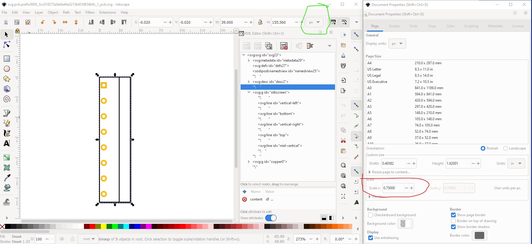
drawing units of the svg editor that made the svg. In a properly formatted Fritzing svg (which many, even in core parts, are not!) that is 1 unit = 1/1000 in. The easy way (although you need to learn Inkscape or another svg editor) is to edit the svg in an svg editor like this (the pcb svg for the Camdenboss CTB0158-8 connector)
here the scale is incorrect (it should be 10.41667 to put drawing units in 1/1000 of an inch) which will mean drawing units are in some odd value (which Inkscape will convert to in when required!) By default the tool bar units are px (96DPI in this version of Inkscape) but can be changed to in which sets the tool bar coords to in.
That said, learning to use Inkscape isn’t easy, and Fritzing adds some complications (Inkscape adding px to font-size which Fritzing won’t accept correctly is one) so you need to post process the svg to make it acceptable to Fritzing. FritzingCheckPart.py will do that for you (as well as check the format of your part), and is available here:
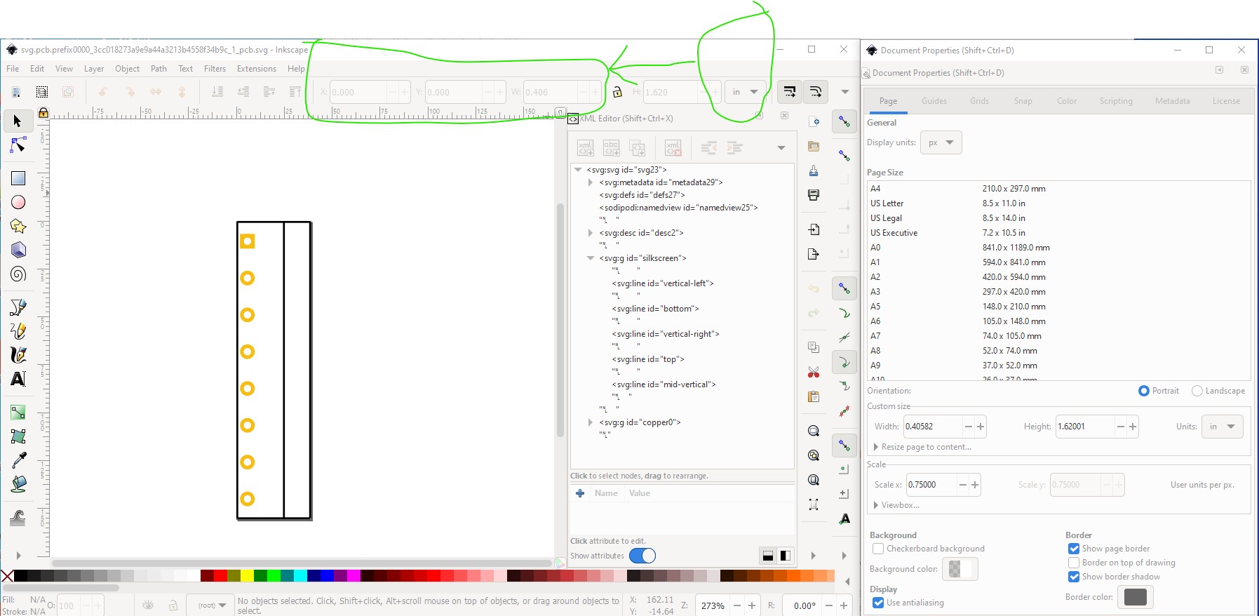
It is almost as complex, but deterministic. It is scaled from the viewbox setting by a formula that I don’t know (but is undoubtedly in the svg spec) to set the drawing units. In this case as well as the incorrect scale, the document start coords are slightly offset. The starting x and y should be 0 not -0.020px.
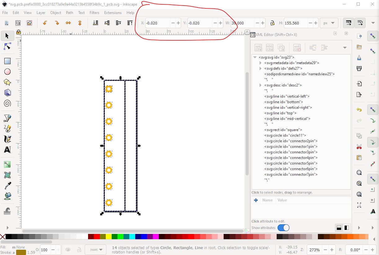
So I corrected that then rescaled the drawing in Inkscape to get drawing units in to 1/1000 of an inch to create this svg
which should now have drawing units in 1/1000 of an inch. If you make your changes with a text editor you don’t need to worry about the px values (there is no text in it anyway!) Right click on the svg image and select save file as should download the svg. I can easily enough make the changes need to silkscreen for you as well and create a new part. That way you have a working part to compare to your changes.
edit:
Since it is easy for me to do, here is a corrected (I think!) svg
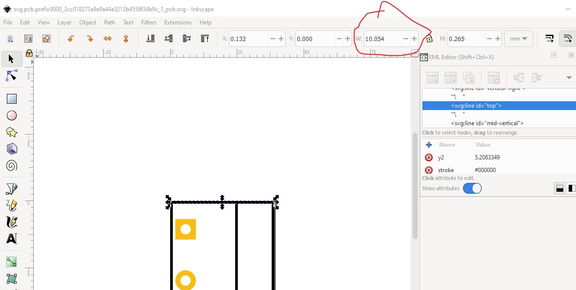
Note the original svg appears to be slightly wrong in that the horizontal distance is set to 10.054 when the data sheet says it should be 13.8mm.
you are awesome. thank you so much. and for the svg too. this all makes sense. i will play around with it all now and post back if i have anything interesting to share.
One additional (but important!) note on units in the svg: if you see a transform (typically transform translate set of numbers) the drawing units there after are modified by the transform matrix and thus are no longer in drawing units (at least not in untranslated drawing units.) That doesn’t matter in my svgs because they have no transforms, but parts editor loves groups and transforms so you may run in to it in svgs from the parts editor.
so i haven’t got to the 0108-8, but i’ve been messing around with inkscape (and also found it was way easier to just use the xml editor or notepad, because inkscape kept nudging coords around when i edited sizes – probably just user error on my part). one thing that i learned that kept tripping me up is the stroke is centered on the edge of the shape; so it must be accounted for in e.g. circle radii and rectangle dimensions.
i was also able to get the svg units to be in mm and they work in fritzing. i was also able to remove those transformations you mentioned (thanks) which helped a lot.
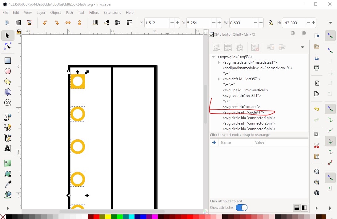
however, messing around with the 0158-8 I noticed numerous issues with the part itself. there was the dimensional issues you pointed out and also the hole size was way smaller than the datasheets recommended minimum size (1.5mm diameter).
so here’s an svg for a fixed 0158-8, with increased hole size, and – since it’s a rather large part – a 0.4mm annular ring (which satisfies aisler’s 0.2mm minimum as well as ipc-7251’s mmc (max joint robustness) recommendation of 0.25mm. i’m assuming pin 1’s position was correct in the built-in part, though.
i’m curious if anybody ever actually used fritzing’s built-in 0158 connectors with good success, given that the hole size was too small.
here’s the graphic:
i’m not really sure how to fix the other variants in fritzing without modifying each one individually. fritzing is a bit klunky here because really the hole and pad sizes are properties of the part family and the project itself, not the individual part, so there doesn’t seem to be a good way to change design requirements besides making an entire new parts library…
here is a corresponding fritzing part (i updated a bunch of the metadata too):
while the recommended hole size is 1.5mm the actual pin appears to be .9mm and it is possible that the current hole size is big enough that it fits in most cases. The current part hole size is 0.04in or 1.016mm so the pin should fit (although perhaps tightly!) The recommendation may be for automatic insertion equipment which likely needs more clearance.
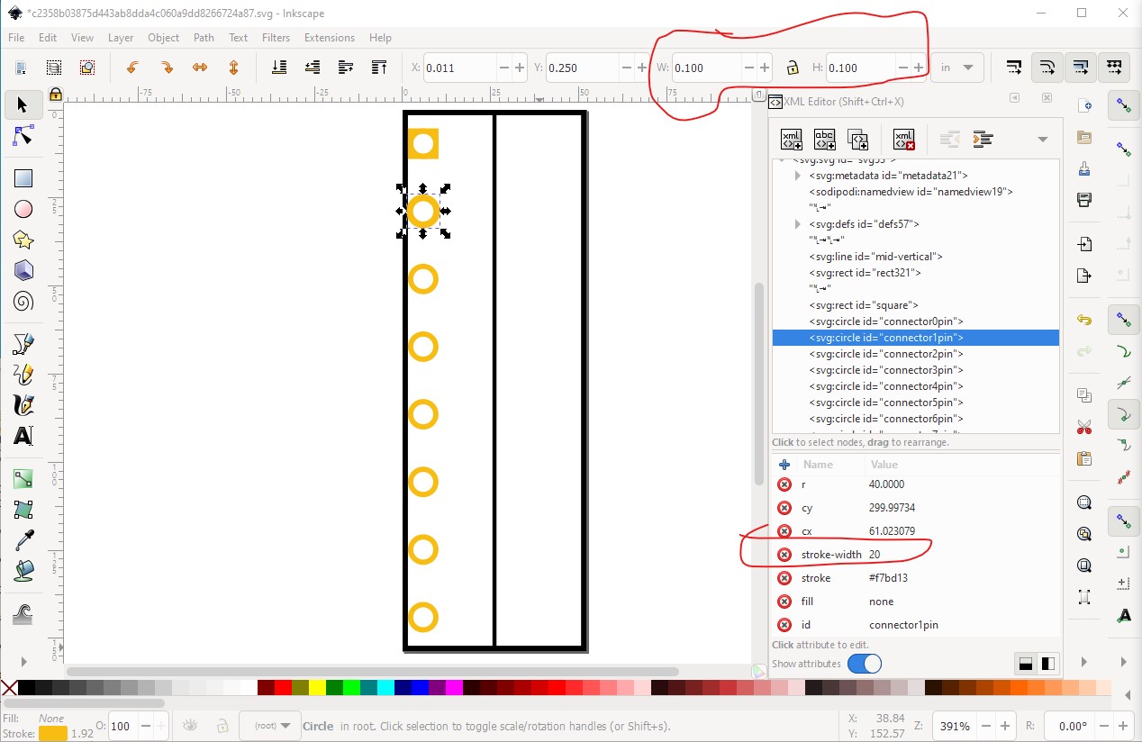
The standard in Fritzing for ring size is 20 thou (so 0.508mm). Which makes a little bit larger ring which is likely better. In Inkscape the hole size is set by
hole-size = pad-diameter - (2 * stroke-width)
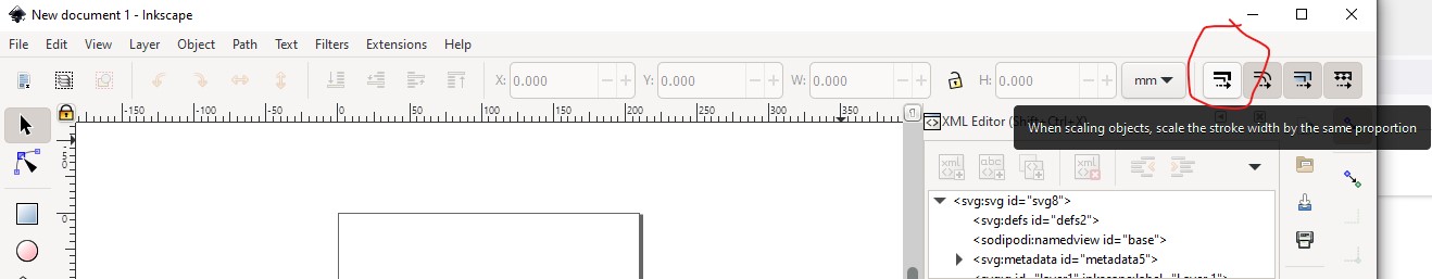
As to your problems with Inkscape changing sizes, there are two possibilities, one is if you have scale stroke width (the button circled in red in this image) which changes stroke-width when you increase the length of an element. I think it is on by default and I usually shut it off. That doesn’t entirely clear the problem though as stroke-width factors in to it in some circumstances. Then changing the coords multiple times to the values you want a couple of times converges on the values you want. You can also choose geometric mode in preferences, but it does something else undesirable that I don’t currently remember so I just live with it as is.
but when you ungroup the connector name is lost. It is preferable to set it on the circle that is the connector as that won’t get changed in an ungroup. As well copper1 should be the first group (because it is the only group in a SMD part) with copper0 under it. I believe either way will work though.
Here I rescaled the svg and set the stroke-width to 20 (20 thou) then changed the pad diameter to 0.1in giving a 0.06in hole which gets the ring size to the standard 20 thou. In Inkscape the way to do this is to change the pad diameters in the tool bar and note the new radius value in sml editor, then undo the two size changes to restore the old pad (because the size increase is from the left edge and top moving the center of the pad) and replace the radius with the new value (which increases the size of the pad from the center leaving it in the same place.)
Modifying the individual parts is indeed the only way to change this at present. There are a variety of suggestions for changes now that development is running again, but so far changing all the parts is it. It may need to remain it as the hole sizes in pcb are set from the pcb svg and changing that may be too difficult. we will have to see.