Is anyone working on Parts for the SK6812 range of RGB LEDs?
I’m i need of the 3030 package, 4020 package and the mini E package please.
A quick look turns up a data sheet with a single package outline.
but not any of the others (nor is it clear which package this data sheet is for.) If you post a pointer to data sheets for the packages you want it is easy enough to change one of the current led parts to match.
Peter
SK6812 4020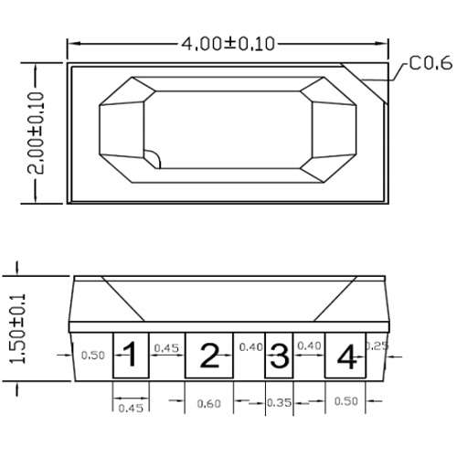
SK6812 mini e SK6812 Mini E
Still problems. The 4040 version has no SMD pad dimensions, it has the pitch but not the size of the pcb pad it connects to.
There is a mini data sheet here:
but it doesn’t have a recommended pcb footprint, and is odd enough that the foot print must be correct to avoid shorts on the pads (and the pads may need to cover the entire pin for heat dissipation reasons.) It also doesn’t agree with with the mini image you supplied (which in turn looks to be for a connector, not smd, it looks like the pads are above the plane of the board and won’t connect for SMD soldering.) So still not enough data to do anything. I need the sizes and positions of the copper squares for pcb for each package like this (from a different led):
each square needs x/y position and height and width to know what size to make the pads. They are often also used for heat dissipation and thus need to be of sufficient size.
Peter
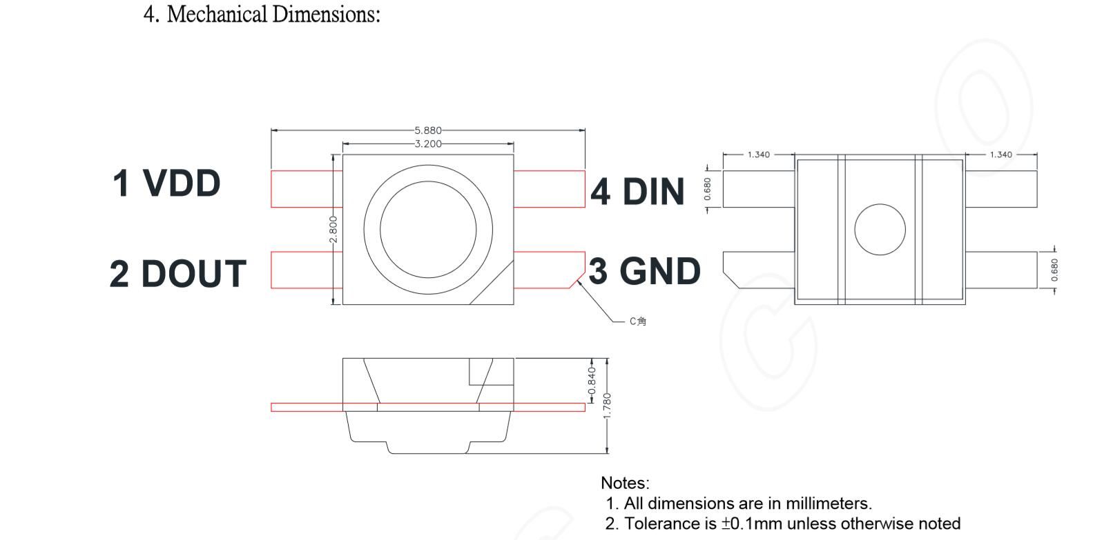
The pads marked 1 - 4 on the 4020 are SMD pads. The diode looks strange because its a side exit diode and not a top exit diode.
Pad 1 0.45mmX0.6mm - DIN
Pad 2 0.6mmX0.6mm - VDD
Pad 3 0.35mmX0.6mm - DOUT
Pad4 0.5x0.6mm - VSS
That does for the 4020 version, how about the mini? Is it SMD or does it want a connector (which is what it looks like?) If it matches the adafruit data sheet, which way are the pads oriented? It isn’t clear if the footprint data is looking from the top or the bottom (and that matters to the footprint.) I don’t have one to look at to tell which way it should be. The pcb footprint needs to be from the top looking down as the LED will attach to the board.
Peter
Ahh sorry, I mis understood. Its actually got legs where there should be pads on the base. It is designed to be soldered poking through a hole from the underside of a pcb.
Top down pinout
1 (Top Left) = DOUT
2 (Bottom left) = VSS
3 (Bottom right) = DIN
4 (Top Right) = VDD
All legs stick out 0.68mmX1.34mm with the exception of VSS which has a 0.34 chamfer on the outer corner.
1 big issue i have found is 2 conflicting mirrored pinouts.

Which has the pinout as
1 = VDD
2 = Dout,
3 = VSS/GND (tapered pin)
4 = DIN.
Again, sorry, I’m a new user (well actually lost my details years ago) and so stuck to the 1 pic per post limit.
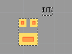
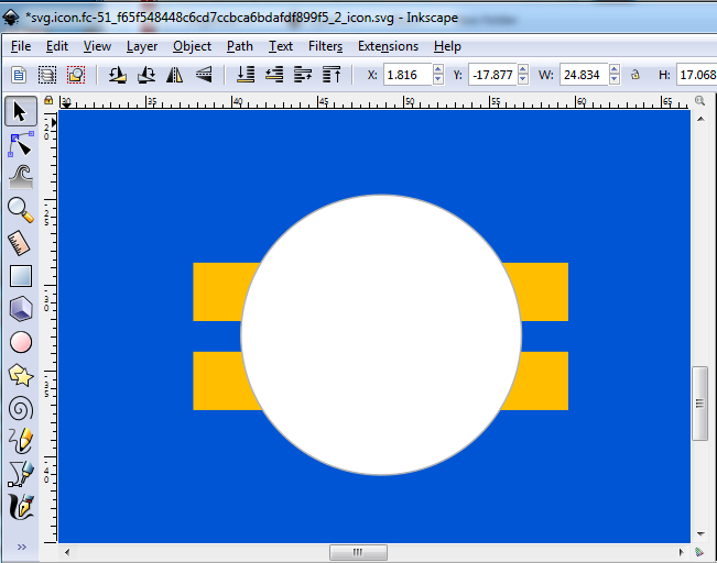
It is entirely possible this is the same part one with view from the top and the other view from the bottom (of course with no labels to tell you that.) This is very common (and very frustrating) in data sheets. I think illumination has struck, this looks to be one of the so called middle parts (usually USB connectors) where the body fits through a hole (or rectangle in this case) which the led drops in to. That is a problem in Fritzing, because it doesn’t easily support rectangular holes (and as far as I know neither do the inexpensive board houses.) Essentially this (the top image is side view and the bottom the board in blue the pads in gold and the hole in white:
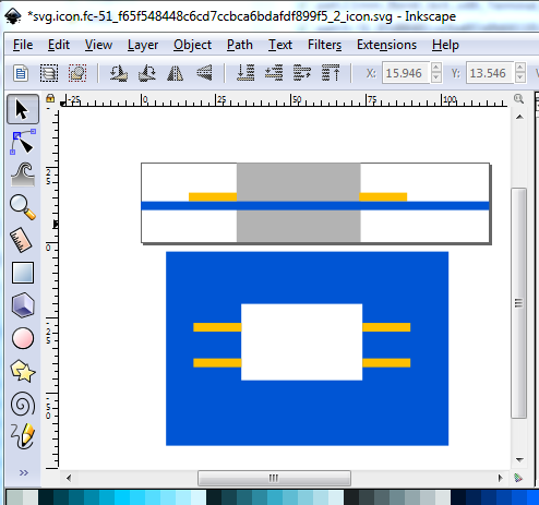
the hole is the hard part, both in fritzing and to get someone to produce it I think. A circle is easy both in Fritzing and for the board house, but I expect it will cut in to the pads to be big enough to fit the square body. This might work (the pads are to scale from the data sheet above) although you are losing about 1/4 of the pad area to the hole(which has to fit the corners of the rectangle as shown):

The footprint will actually look like this:
Peter
Thats interesting that they cant handle square holes, I was looking to add round (well ovalish) in a future version.
Thank you for working on this for me.
I am not anywhere near a pcb expert, I make very few boards, but this discussion has come up before and generally odd shaped holes in boards need gerber layers Fritzing does not generate and most of the cheap board houses don’t support.
edit:
OK, this part should do for the -4020 part:
edit2:
replaced the 4020 part with an improved one (added a data sheet url) and a mini part. The mini part may not be correct because it was build from the drawing in the pdf in the data sheet so it really needs to be checked against a real part … I can find no data (except people that will sell me any number) of the 3030 part.
SK6812-4020.fzpz (7.7 KB)
SK6812-mini.fzpz (7.9 KB)
You need to verify the pin numbering in pcb against a real part. The pads are .1mm larger than the stated pad width to give a little bit of misalignment room.
Peter
1 Like
Thanks, once I order some “real” parts I will compare and let you know.