I have a 2.8-inch SPI TFT Module with PCB board dimensions of 50 x 86 mm. I want to interface this PCB to the Arduino UNO PCB with a shield like connection. The UNO PCB has dimensions smaller than the display PCB. I want to connect this 2.8-inch SPI TFT Module PCB to the shield PCB using a 14-pin socket header.
I am venturing into a more advanced layout problem. I would like to “assume” that if I use a Fritzing PCB with dimensions of 100mm long x 80mm high, and drag the Fritzing Arduino UNO part onto the larger Fritzing PCB.
Then, according to the details of my Fritzing PCB drawing
everything will fit together as shown in the attached Fritzing file.
Under these assumptions, the UNO part will locate the plated thru holes onto the proposed shield PCB.
When I design this shield PCB in this manner, I expect that the Gerber file generated will produce one PCB for the shield PCB with the PCB plated thru holes generated by the UNO PCB part and the 14-pin socket header.
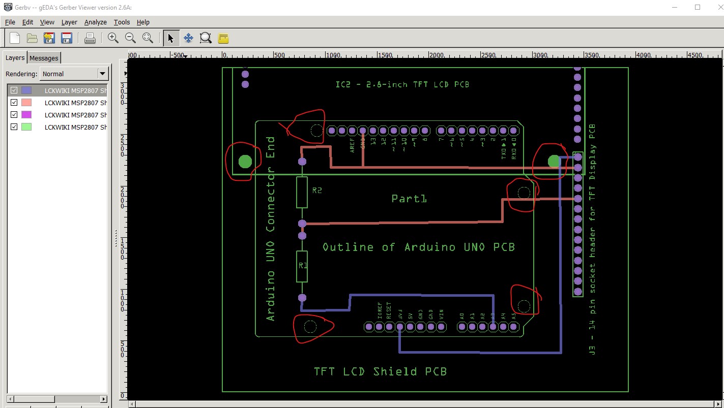
I see a couple of issues here. This was created by exporting pcb from your sketch via File->Export->For Prodution->Extended Gerber then loading copper top, copper bottom, drill and top-silkscreen layers and displaying the result with the gerbv gerber viewer which looks like this:
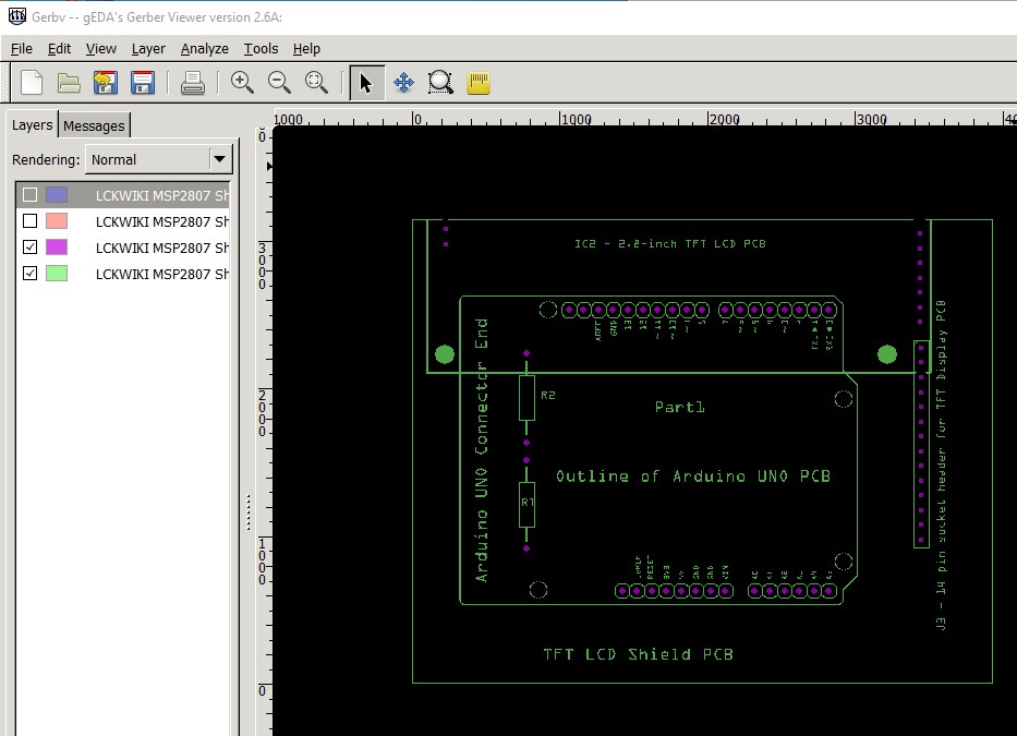
The issues are none of the mounting holes are being drilled. This is a Fritzing oddity, they are only in silkscreen in case you don’t want the holes (you need to modify the part to remove them but can add holes to your sketch if you want the mounting holes.) If you do want the holes you need to drag the core parts/pcb/hole over the hole in silkscreen and set the size correctly to drill the holes. Here I suppressed copper bottom and copper top leaving only drill (purple) and silkscreen (green)
as you see the mounting holes are only on silkscreen and won’t be drilled. As well on two of the mounting holes, the traces are too close and will likely be cut by the drill. You need to move the traces away from the mounting holes. I am assuming wires will run from the display to the pads on the pcb, in which case what I would do is drag a hole (after moving the traces to clear the holes which I have done here) in to the sketch:
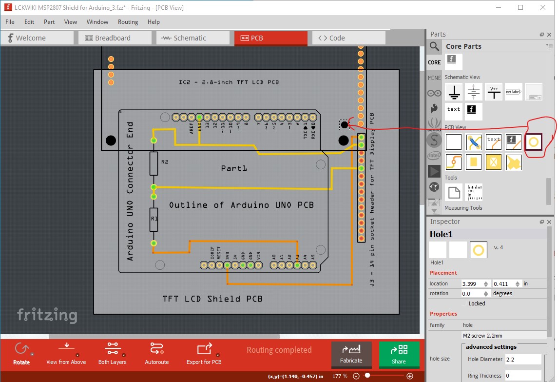
increase the hole diameter to 3.4mm and drag the hole over the hole in silkscreen. Do the same for the other hole, then delete the TFT display to get rid of the unwanted pads but leave the mounting holes which will now be drilled.
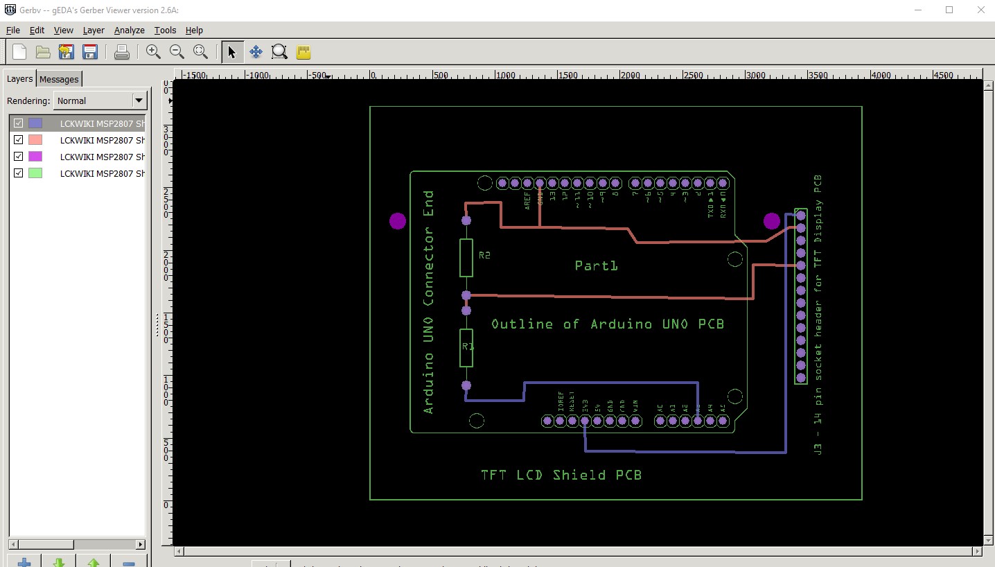
Peter: Thank you for flagging these issues. I was planning to add the holes using the display PCB for reference, and address the trace routing as a final layout step.
My question relates to lining every thing up using this procedure in order to produce one large single shield PCB, using the Fritzing UNO model to locate the shield holes in order to connect to the Arduino UNO PCB and to connect to the display PCB.
Yes it should. You will get the Uno pads (essentially everything shown on the gerber output) and the copper traces connecting to the header pins that then connect via wires to the LCD display. You can then solder either male or female headers in to your pcb and they should connect to the corresponding connectors on the Uno just like any other shield. Changing the side of the board the headers are attached to allows either mounting your board on the top of the Uno or (with the headers on the other side of your pcb) the bottom of the Uno. One additional note (although it may not matter in this case) is that both the Uno and the TFT display are on the top of the board. The reason that may not matter in this case is that the mounting holes should work fine if the TFT wants to be on the bottom of the board (for instance to avoid the UNO) if you have pins from the TFT that would matter but with wires it doesn’t.