I want to do a single-sided layout, but it looks like you can only use the bottom layer when the PCB is set to single-sided. I would like to use only the top layer, so that I don’t have to “think upside-down”. Is this possible?
No, but I’m not sure what “think upside down” means in this context. The board will look as normal with the components on the top of the board and the copper on the bottom of the board just as if it was 2 layer. The only difference is that the copper is on the bottom layer only (there is no top copper layer.)
Peter
If you are looking for single sided SMD, try clicking “View …Above” on the bottom bar. That changes to “View …Below”. Now, if you set in inspector (for each part), pcb layer bottom, I think everything will be as you want.
That will setup to view the board from the bottom, and put both the traces and parts on the bottom.
I think a little bit more information on what you are trying to achieve is needed here.
If you are using THT components, then this doesn’t make sense, as you would want the copper on the bottom of the board. If you are using SMD, then yes, you only want copper on the top of the board. What are you using?
You can view the PCB from the top or the bottom, so no need to ‘think upside-down’ because you can ‘see upside-down’. You can also, using a double sided PCB, set it so that only copper on the top or bottom side, can be worked on. Both of those settings are in the bottom toolbar in the PCB layout view.
Please explain further what you are doing…
Randy
Thanks for your time and responses.
Please explain further what you are doing…
I’m working with SMDs only, and I’m doing single-sided copper because I’m etching it at home with Ferric Chloride.
If you are looking for single sided SMD, try clicking “View …Above” on the bottom bar. That changes to “View …Below”. Now, if you set in inspector (for each part), pcb layer bottom, I think everything will be as you want.
This is the best solution, but far from ideal, as explained next:
I’m not sure what “think upside down” means in this context
What I meant with “think upside down” was that if I use a solution like this, I have to keep a mental note that bottom is actually top, and top is bottom. I’m bound to accidentally mount some edge connector upside down if I do this.
I will admit you seem to have found a use case that I don’t think has been considered. What you want is to be able to have a single side board with the copper on top (for SMD) which isn’t a current option. As pointed out, “view from below” mostly works, the exception is silkscreen. Silkscreen is on the top layer and thus appears backwards in this view like this:
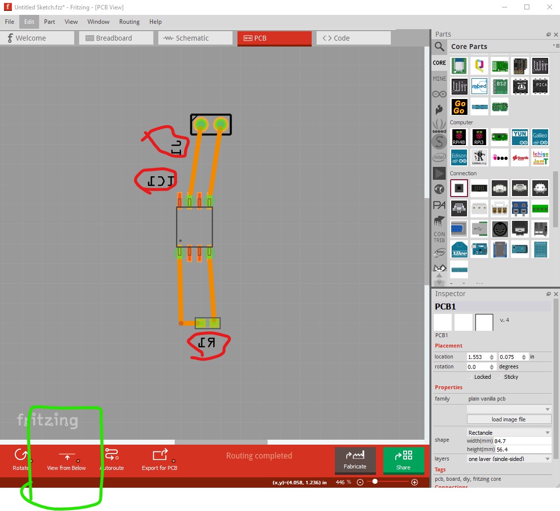
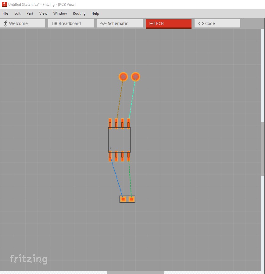
here I have set a single side board and view from below. That means the IC and resistor are shown how they will be on the board viewed from the top. As you see the silkscreen text is backwards. As to connections to connectors, if you start from schematic view and make all your connections there like this:
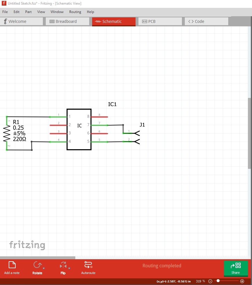
then switch to pcb view
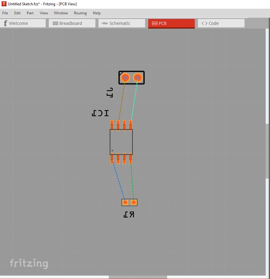
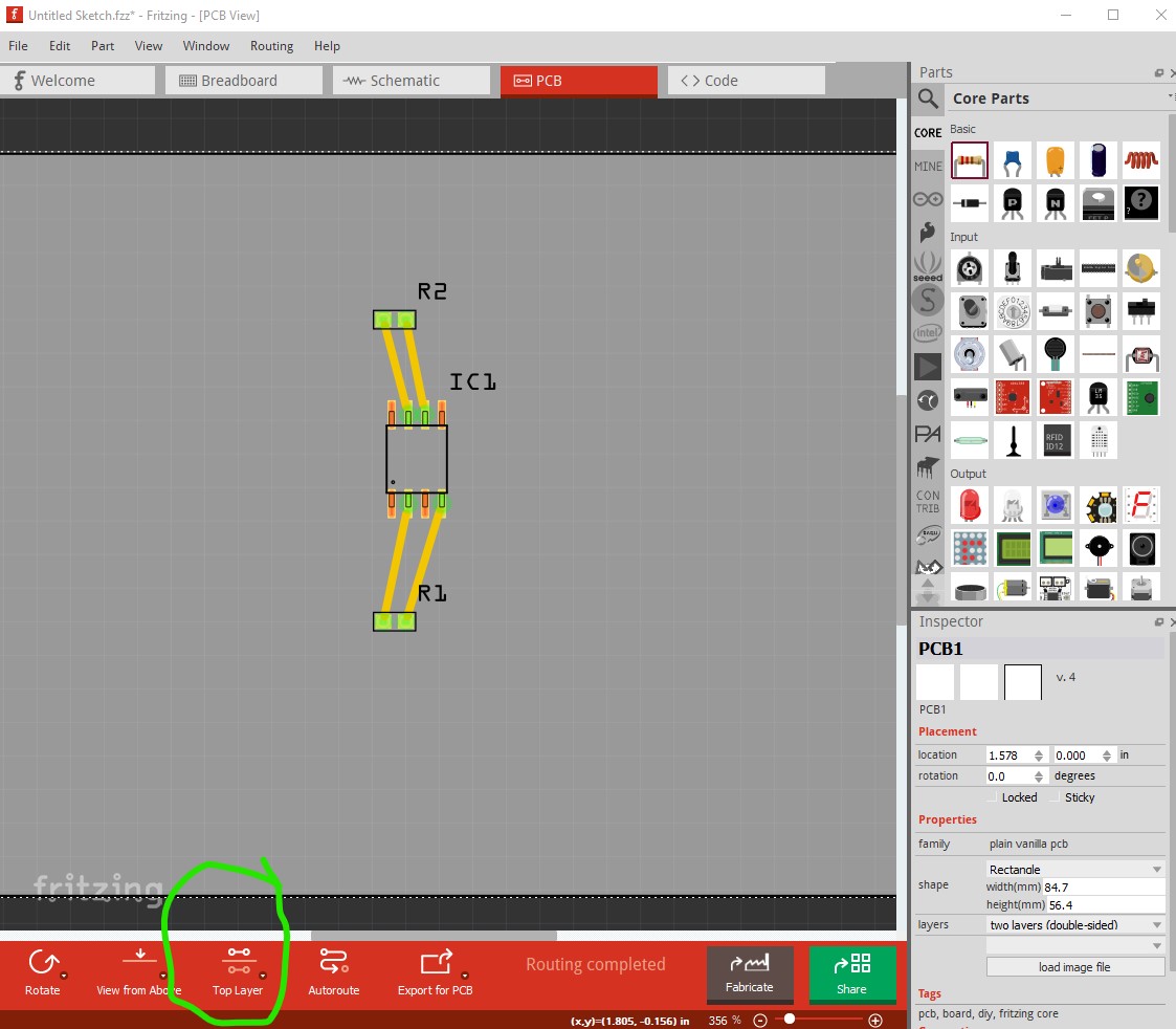
the connections to the correct place are shown by rats nest lines and clicking and dragging on them will turn them in to traces which should fix your issue I think (but at having to wire the circuit in schematic, which I usually do anyway but may not suit you!) I think that is as close as we can come for now. If you don’t care about the silkscreen text (which you may not) you can suppress it by unclicking the top silk screen layer here:
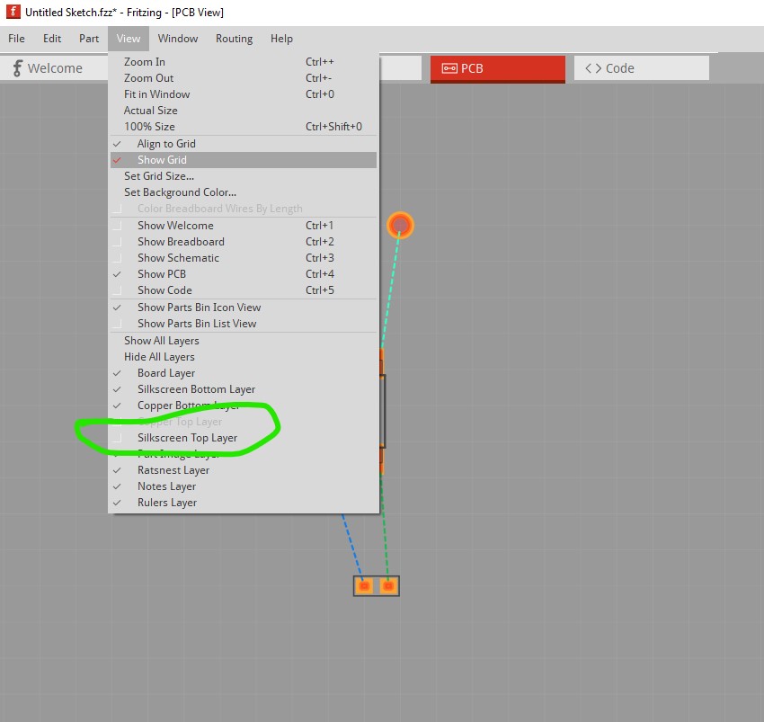
which suppresses the text and reduces the clutter.
and perhaps gets you closer to what you want.
Peter
@vanepp That’s a very detailed analysis  Thanks a bunch.
I think I’ll do this specific project in KiCad after all, but I’ll definitely return to fritzing for breadboarding and especially working with stripboard. (Most of my projects end up on stripboard, if I can find everything in through-hole form.)
Well that is “curious”. This is mixing view from below and single sided. If I leave the board set to double sided, and set view from below, it works cleanly. New parts added to the sketch are placed on the bottom, and silk screen is added to the bottom and displays correctly. Switching to single sided, and placing another part goes to the top, and silkscreen on the top and displayed backward. Moving the part to the bottom leaves the silkscreen on the top and text backwards.
This needs more testing, to see what gets through to gerber, but it “appears” that the best current process is:
- before adding any parts to the sketch (in any view)
- set the pcb to double sided
- set pcb view from below
- place all of the needed parts (any views)
- set the pcb to single sided
- do the pcb trace routing
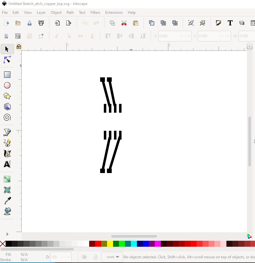
I think even this will be a problem. The board will end up with the SMD parts on the bottom layer and thus inverted horizontally from where they need to be to be on the top of the board. You could use Inkscape or another image editor to swap the output image horizontally although that is an extra outside step! It also doesn’t work, although I am not sure exactly why. The flip horizontal moves the position of the resistors which is incorrect. This svg is the top layer output of a 2 sided board routed only on the top:

this is the copper bottom svg flipped horizontally from a single sided board

the pins connect correctly but the location of the resistors is wrong. I think the answer that may work best is to select a 2 sided board, set “route only on top layer”, then only use the output for the top layer (as it should be in the correct orientation) and ignore the bottom layer output (which should only have through hole parts pads and no traces.) Doing that I get this:
Where the copper etch output matches what I see in Fritzing.Ideal would be an enhancement, to be able to select a single sided pcb with the single side being the top, but I don’t know how big a code headache that would be. Maybe a big one, as I expect the current situation, single side is always bottom is probably the base assumption in many places (and even worse perhaps an implicit assumption in places that are not obvious!) There doesn’t appear to be a simple solution I don’t think. Before this post I hadn’t considered that someone may want a single side SMD board (with the implied copper on the top of the board), but it makes good sense, I’m now surprised this hasn’t come up before to my knowledge ![]() Fritzing is just poorly prepared to produce it.
Fritzing is just poorly prepared to produce it.
Peter
I haven’t visualized all of the scenarios, but simply treating the Fritzing ‘bottom’ view as the actual top seems to work. Since this is single sided, there is only one side, with (for SMD) everything on the same side. Parts, copper, silkscreen. Fritzing will call that the bottom, but just ignore that. This is set to view from the bottom, so everything should correctly match between the Fritzing bottom ‘view’ and the actual board with copper side up. The gerber export will also ‘name’ that the bottom side, with the top empty, (and the gerber viewer probably displays from the top) but so what? The board will be produced with the copper and silkscreen on the same side. Once you have the board in your hands, top and bottom are arbitrary.