so when i place a screen print image across an entire board. how to i make it so that the areas where a pad or via are; it will leave an opening through the screen print layer to leave the pad or via copper exposed?
That should happen automatically. Fritzing will exclude silkscreen from exposed copper. You can verify that by looking at the gerber output with a gerber viewer.
Peter
what is a good gerber view. will this show it as a complete 3d board?
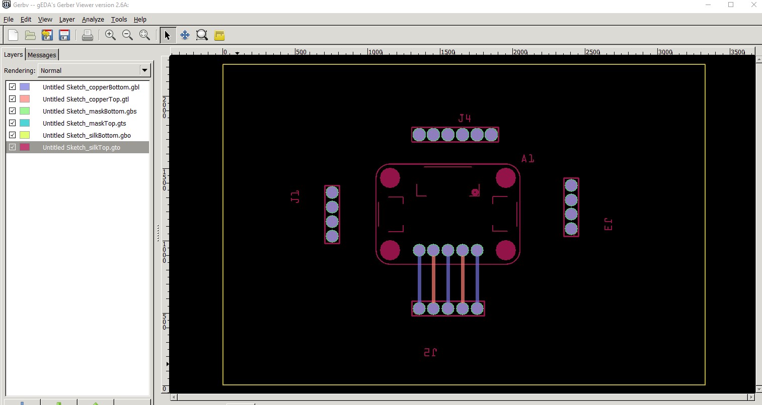
There are a lot of them. I use gerbv from the geda project (another open source EDA package.) There may be some that do 3d views although I don’t know if the gerbers provide enough information for that. Here is the gerbv output from the last thing I generated gerbers for (an Adafruit board) which should demonstrate the output.
First the all layers output
then bottom mask only

then add in bottom copper again to show where the mask will apply
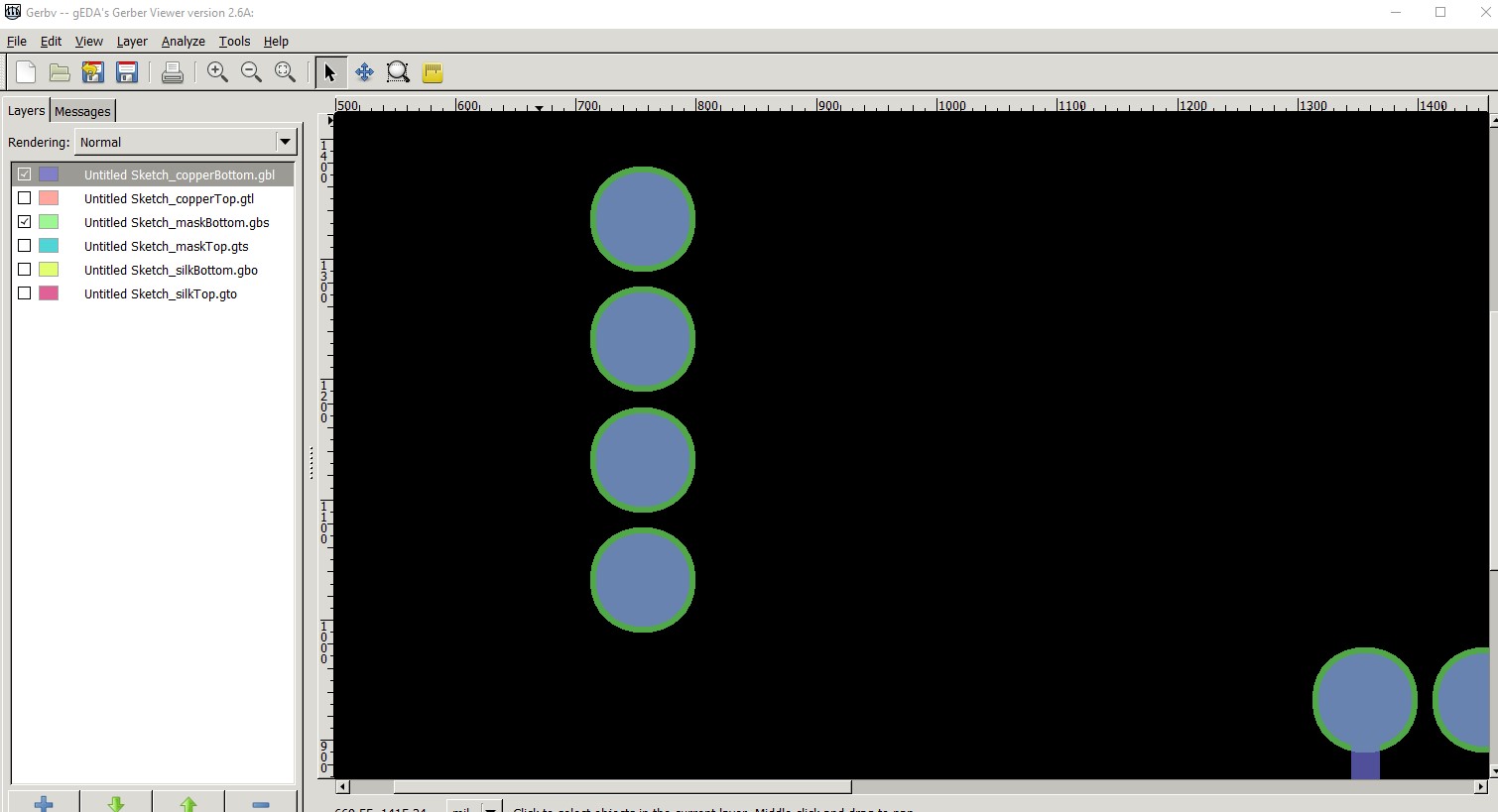
the green overlap here is how much clearance you should get between the mask and the copper (I don’t know of a way to modify that in Fritizng, although there may be one somewhere (I think it more likely needs a code change though.) Hope this helps.
Peter
oh yeah this looks good. i will try that program out