I’m 99% sure this article that includes node terminology has cleared up my understanding, in that connections can be drawn point-to-point (not common), or as the more common ‘distributed node’ schematic and they mean the same thing:
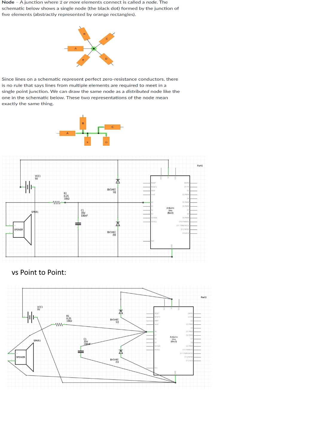
As an absolute beginner, point to point currently works better for my brain - so could someone do a sanity check for me and confirm that these 2 schematics I have drawn are equivalent:
(I can upload the fritzing files if preferred).
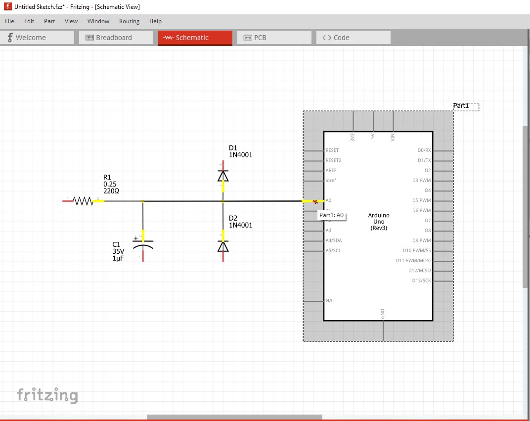
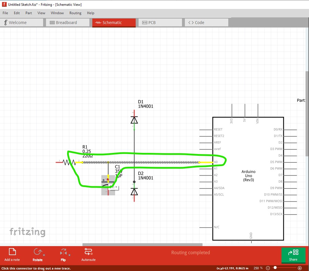
It is preferable to upload the .fzz files for the two sketches so we can see the actual sketches. That said this Fritzing feature will help you do this for yourself. Here I left mouse clicked on the A0 pin of the Arduino. That lights everything connected to the pin in yellow, indicating that, yes this particular set of connections is identical to your split apart image (that doesn’t always need to be true, there are connections which will look the same but not be correctly connected!)
Hi, I’ve uploaded the .fzz files now in this reply.
Could you elaborate on the last part of your last sentence - that “there are connections which will look the same but not be correctly connected”? What might be an example of this?
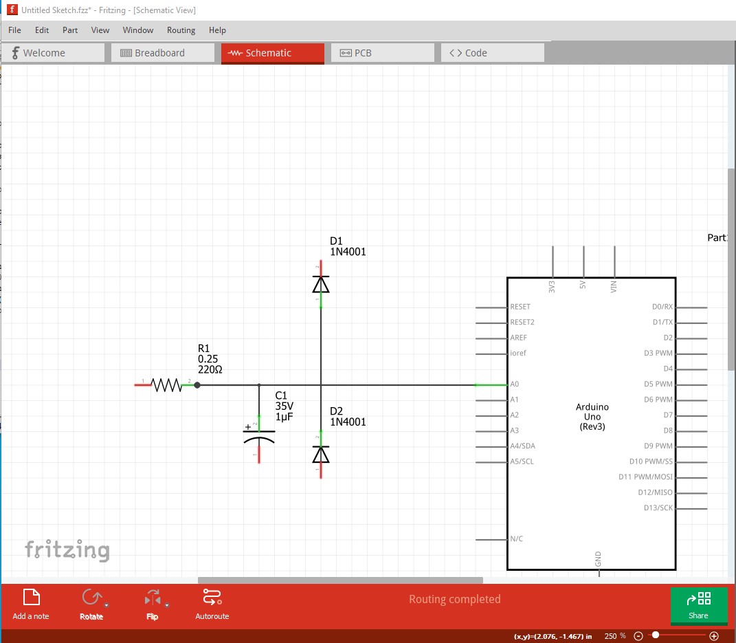
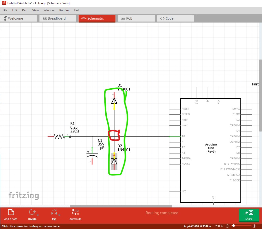
Yes the two sketches are identical. If you left click on a connection the same pins in both light yellow indicating the connections are the same. This sketch looks mostly identical to the original but is not (and is the most common case of this problem!)
the diodes are connected together and look like they should connect to the resistor capacitor and micro pin but in fact do not connect. This trips new users up all the time.
Elaborating a little, it is the difference between these 2 schematic segments. In the group on the left, the wires “connect” in the middle. For the group on the right, the wires “cross”, but do not connect. Visually the only difference is the “dot” where they connect, but not where they cross.
You can also get caught by the routing of wires. Consider these 2 schematic segments. They have exactly the same (end point to end point) wire connections. The one of the right though has the bends in each of the wires at exactly the same point in the middle. Both of these are electrically (on schematic) equivalent to the left example above, but the dot for the bend is smaller than the dot for a connection. Making it hard to tell apart from the right diagram above. Where practical, route wires to avoid crossing where there is no connection. That is not always easy (or even possible). You should though always be able to avoid routing wires and bend points directly on top of each other.
For more advanced cases, real wiring like this (on PCB for example) should be avoided. It creates a ‘loop’, which can cause strange effects because the wires are not actually zero resistance.
Uing the “left click”, you can always get Fritzing to show which connectors are actually connected. Where parts have internal connections (bus) defined, that can show things connected where there is no wire in the schematic. For example, there is an invisible wire between the 3 separate ground pins on an Arduino Uno board. That does not show in schematic, but does show on breadboard view. Other parts might have multiple pins in schematic view that are invisibly connected.
Thanks for the insights. I think I’m getting a better understanding - particularly around trying to think less around something ‘flowing’ from one component to another - instead components in the same node have equivalent voltage and current all at the same time.