Hello All!
I’ve tinkered with electronics for a few months and I’m totally hooked! I’ve mainly been working on creating remote controlled cars with different types of Arduinos and NRF24l01 transceivers. I’ve successfully created a couple different breadboard designs and decided to try and create a custom PCB for the remote transmitter. I hope to make the car receiver PCB in the future. I’m a complete beginner at PCB design and I would love some feedback.
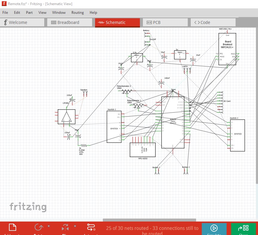
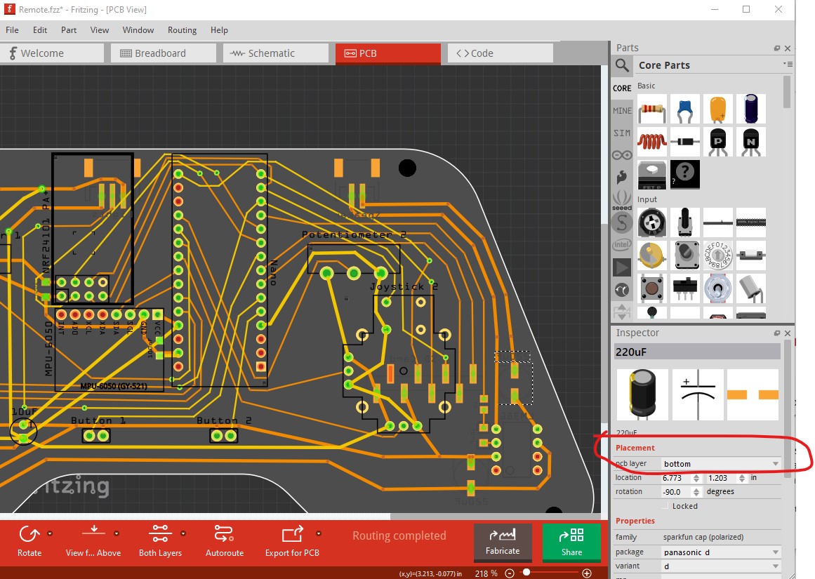
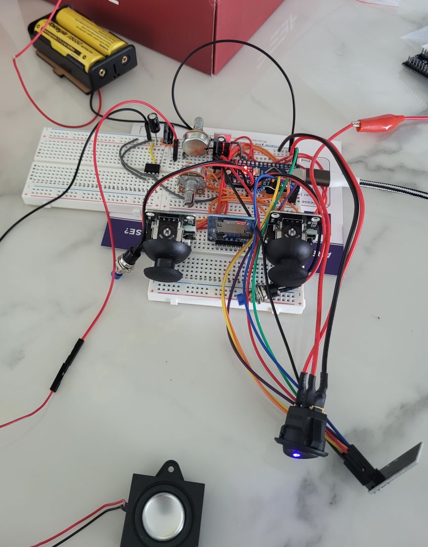
Here is a description of the remote. The 3 JST connectors will go to an 18650 battery pack, a WS2812 with 10 LEDs at half power and a small 8ohm 1 or 3W speaker. I plan on using an NRF24l01 as a transmitter and take user inputs through 2 10k Joysticks, 2 10k potentiometers to control servos, a gyroscope for tilt controls and 2 buttons for sounds/music. There will be an SD card for playing sounds that are triggered by different events. I will have a plastic cover attached to the drill holes on the 4 corners to protect the electronics and mount the battery pack, speaker and lights to. I’ve laid this out on a breadboard and tested all the different components successfully (minus the lights).
Remote.fzz (51.4 KB)
Here are some newbie uneducated questions and concerns I have with my design:
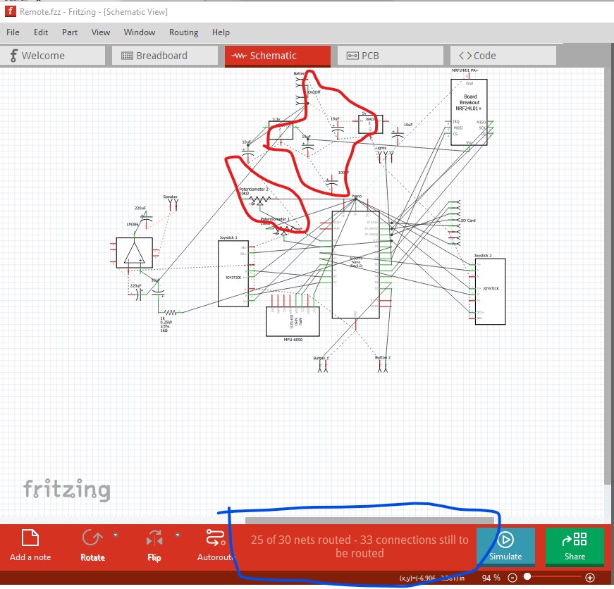
1.) I’ve been watching some PCB design videos and had a question about ground planes as it relates to my project. I routed all my ground connections but can I just do a ground fill and remove all my routed ground connections with no issues in my design?
2.) If I do a ground fill, I’ve watched some videos about how the return path for high frequency signal traces don’t use the shortest path but instead use the space below the trace. I tried, as much as possible, to not interrupt the space below traces and run most of my signals on the bottom layer but couldn’t leave the top layer 100% empty for the ground plane. Do you think I will run into issues with signal integrity due to the crossing of traces with my design?
3.) Also on the topic of EMI, I’ve heard about crosstalk in traces with long parallel runs. I have some parallel runs but tried to space them out. I’ve heard a rule of 5x the width of the trace in spacing but I don’t think I could achieve that with my board size. I also tried to keep my power traces on the outside of the board but had to run a power connection directly to the Nano in the center. Do you think I will have crosstalk issues with my design?
4.) I added a separate 3.3v supply to power the NRF because I’ve rarely been able to get the NRF to work from the Arduino’s 3.3v pin. I also read the datasheet on the regulator and it suggests a 10uF cap on the input and output of the regulator. Since this is the only device I’m powering with that 3.3v source, do I still need the 10uF cap near the NRF or will the 10uF cap from the regulator suffice?
5.) I plan to use 2 18650 batteries to power everything and that gives me a nominal voltage of 7.4v. Is there any power supply filtering I should be doing outside the caps for the voltage regulator? I added a 100nF cap near the Arduino but I think there is already a 100nF and 4.7uF cap on the 5v pin. Do I need my 100nF cap in that case?
6.) I plan to play sounds for different events that the car may have using an LM386 on the remote. I’ve gotten the LM386 to work pretty well with the design I put on the PCB. I noticed that I didn’t need to increase the gain by using a cap across pin 1 and 8. It’s really loud already and the volume setting in the TMRpcm library gives me plenty of volume. Do you think the proximity to the SD card will cause any issues like clicking noises while the SD card is reading?
Any other advice or criticism is very welcomed!