Still some problems. Schematic is I think at 90dpi (because fritzing aligns it to the grid correctly) but it loads in Inkscape .9.2.1 as too small (because it thinks px scale is 96dpi I expect). This is happening because the view box height / width are in px. The solution is to (assuming it loads in your editor at the proper scale) change the view box height and width parameters to in or mm. To do that edit->select all then change the tool bar to in or mm and copy the height and width parameters (in in or mm) from the tool bar in to the height and width parameters adding a trailing in or mm to the value in the first element of the drawing using xml editor. When you press set it will rescale the drawing to the real world coords which avoids the px confusion. For reasons I don’t understand your terminalId definitions are being ignored (that is why the schematic lines in the sketch below terminate in the middle of the pin). That said the correct terminalId values appear in both the fzp file and the schematic svg. Ah! just saw it, your terminal ids are mostly paths (which don’t work as terminalIds. The couple that work are polygons which do work although I prefer a rectangle with height and width at .01 in. I don’t think fritzing can calculate the center point of a path to know where the center should be so it defaults to the center of the pin (which isn’t what you want).
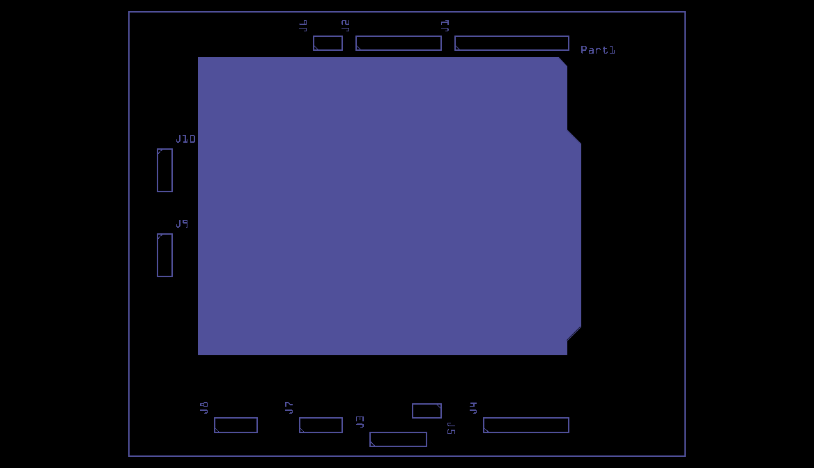
PCB has a couple of problems: the holes for the pads are .035 (IC size) they should probably be .038 (.1 in header post size). The board outline (which I think is one of the polygons) has a fill value set. It probably wants fill:none and a stroke width (although I don’t know how to do that on a polygon) to draw an outline around the board. As it stands the entire silkscreen layer is one color (the fill from the polygon) and the lettering is wiped out. Isn’t parts creation fun  Below is a test sketch that shows the pin alignment problems in schematic (and an easy way to test that the pins all have correct terminalId defiintions.)
test.fzz (75.4 KB)
and this is the output from the gerbv gerber viewer of the top silkscreen layer
you can see the correct outlines of the connectors I added, but all the text on the board is washed out by the board outlinel
Peter