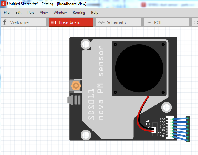
Welcome to Fritzing! Your part is pretty good, it works in all views (many submitted don’t ), it does have a few issues though, from the data sheet the connectors should be on .1in centers (like a .1 header) but in your part they are not, they are smaller than that. It is preferable to align the pins on the .1in grid. There is also a pin sequence problem connector3 is missing (the connectors should run from connector0 to connector6 not connector7.) It looks like you have used a 2mm 7 pin connector in breadboard, changing to a .1 pitch connector fixes this problem:
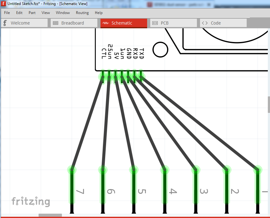
The wires from the .1 header should be straight in to the connector on the dust sensor if it is 0.1in. In schematic you are missing terminalIds on the pins. This causes the wire to connect in the center of the pin rather than at the edge as is desirable. As well again the pins are not on .1in boundaries as they should be in schematic (to match most other parts):
pcb is spaced correctly on .1 centers, but the holes for the pins are too large at 0.044in where (as you see from the .1 header part below it in this gerber drill.txt output) it should be 0.038in
; NON-PLATED HOLES START AT T1
; THROUGH (PLATED) HOLES START AT T100
M48
INCH
T100C0.044221
T101C0.038000
%
…
I fixed up all these issues in this improved part, but I’m not sure the pin labels are correct (the data sheet here does not match your labels, so I used what the data sheet says.) I found what appears to be the official data sheet here:
If you have a different version of the device you may need to change the labels back. I increased the size of the connector in breadboard and schematic to be on 0.1in centers (in breadboard that moved the mounting hole slightly higher to not overlap the connector.) I also changed the order of the pins so that connector0 is now ctl (which shows as pin1 in the data sheet.) and moved the pin 0 rectangle to the new connector0pin in pcb. I corrected the pads in pcb to be standard 0.1 header pads (with a 0.038 hole.) In all svgs I added the missing layerIds by Edit-Select all then group and change the group name to the correct layerId (breadboard, schematic, silkscreen, copper1 and copper0.) This is also a new part (with a different moduleId and files) so you can load both together to compare the two.
 ), it does have a few issues though, from the data sheet the connectors should be on .1in centers (like a .1 header) but in your part they are not, they are smaller than that. It is preferable to align the pins on the .1in grid. There is also a pin sequence problem connector3 is missing (the connectors should run from connector0 to connector6 not connector7.) It looks like you have used a 2mm 7 pin connector in breadboard, changing to a .1 pitch connector fixes this problem: