New here and new to fritzing (why I am in the beginners section :)).
I have done a breadboard design (I have actually soldered this onto a blank PCB and built the software already so I know it works) but I am looking to get a ‘real’ PCB done (outsourced) so looking to sort out the schematic and PCB.
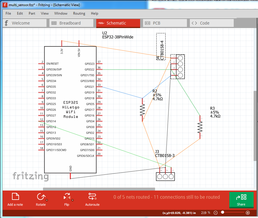
After I built my breadboard I went into schematic and it is truely a rats nest and I can’t figure out how to lay it out nicely LOL. The same for PCB :(.
Any help, ideas, suggestions would be greatly appreciated.
You can rotate the components by right clicking on them and using rotate. Then select a ratsnest line (which will take the shortest path to the associated connection) and drag it to an appropriate position:
Thanks @vanepp. I re-did the schematic - after watching a few videos so that I have a better understanding of how to properly lay it out and to make sure everything works properly
One of things I can’t quite tell if I did it right was the pull-up resistors. It seems like they are right but they won’t “prove” themselves when I click on the positive (3.3v) on the ESP32 ie. the connection stops at the resistor versus all the other connections “prove” themselves.
This time I worked from schematic side versus the breadboard side … I hope it is easier to from schematic to PCB.
Any feedback, ideas, suggestions, corrections - VERY much welcome. I have always just built and then diagnosed any issues. But fritzing seems way better as then atleast I have an idea of how I put things together :). On this particular project I actually want to a PCB made and see how it turns out :).
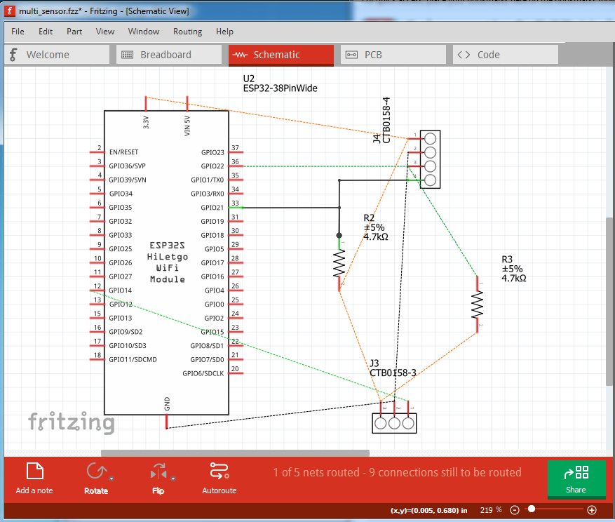
Looks fine to me. If I click on the 3.3V pin on the esp32s all the connections light up yellow (indicating they are correctly connected.) Switching to pcb view you can see the connections as rats nest lines (the one between the two top connectors is hard to see though, as it is under another rats nest line.)
To make seeing it easier I clicked on the rats nest line (which creates a trace) then dragged the one on top out of the way before doing the one we want. Clicking on a point in the trace and dragging will move the trace to an appropriate position as the rats nest lines take the shortest distance to the next connection:
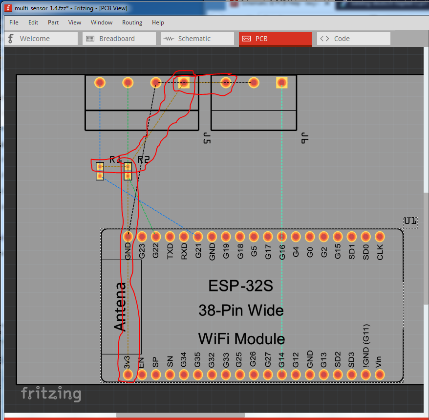
Here the trace on the bottom layer is off the board only so we can see the trace we want between the connectors (the trace needs to be moved on to the board for the circuit to work, if it is outside the gray area, it won’t make it on to the pcb.) Note while it would be shorter to route the trace to the 3.3V pin on the ESP, the box marked antena is actually a keep out area where no traces should be routed as they interfere with the antenna. The standard method of making a turn is to run the trace at 45 degrees on a right angle corner as I did here, it only really matters on rf type traces, but always doing so is a good practice. For something like this right angle corners will work fine though (and are less work to make!) When you finish the board feel free to upload the sketch.fzz file (upload is the 7th icon from the left in the reply menu) and one of us will look it over for problems.
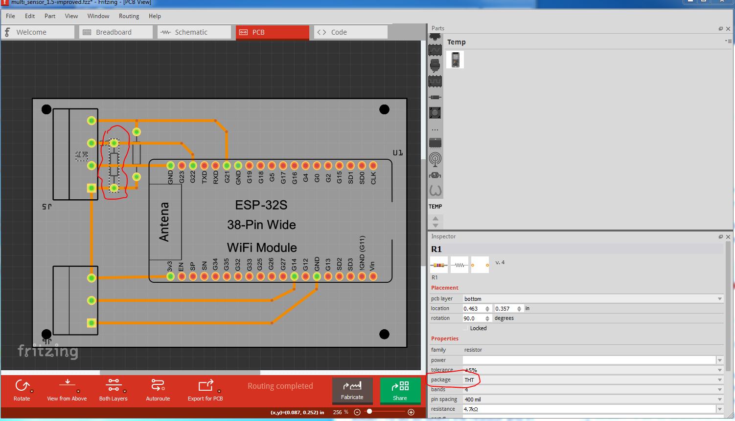
Here is my latest with the PCB ‘finished’. I had a really hard time figuring out how to lay it out without having things ‘cross’. So I ended up having to use some jumpers to make it work.
The other thing I don’t completely understand is which way J5 & J6 (terminal blocks) should face. ie. should the connections be facing the outside of the PCB or the inside (as they are now). Any thoughts on this?
One last questions - when you outsource PCB man. will the company put the resisters, terminal blocks, headers etc. etc. one the board?
Open to all ideas, suggestions, etc. etc. Love learning this stuff :).
Two things you can do about that. The easiest (which is what I did) is change from surface mount resistors to through hole (which are easier to manually solder). To do so select the resistor and in Inspector (the lower right window) change package from smd to tht (tht stands for through the hole) and you can avoid the jumpers.
The other thing you can do is right click on a trace and click “Move to top layer” which will move the trace to the top of the board (as long as the part is not SMD as the resistors were.)
From a look at the data sheet (I don’t have one of these connectors) the screw to connect the wire needs to be facing out from the board which looks to be how it is connected now (you need to make sure that is true though!)
They will assemble complete boards, but normally in 100 quantity I think. The usual (and cheap!) thing is to only get the bare board and do the assembly yourself. That is another reason to not use the smd resistors through hole are easier to solder.
One further question I had. In one of the videos I watched the fellow said to print the PCB view which also showed the holes where things will fit. I wanted to do this to make sure the ESP32 and the terminal blocks fit in the holes. For the life of me - I can figure out how to print that “view” he called it the 1:1?
You can either do file->print with pcb view selected which should print it directly, or file->export->as Image and save the file as one of the formats offered and print that. A third method (and probably the best as this is what the boards will be made from) is export the sketch as a gerber file (file->Export->for production->Extended Gerber (rs-274x) . This will produce the gerber files that will produce the board. The file drill.txt has the size of the drill holes for all the pins and a gerber viewer (I use gerbv from the geda project, but there are lots of them) will display and print the copper layers. The advantage to using the gerbers is that the same data will be used to make the actual boards.
printing “1:1” simply means to print a one pcb unit equals 1 physical unit on paper. That is if something is 1 inch in Fritzing, it prints as 1 inch on paper, so that the size can be matched to the physical parts. 1:1 means “1 to 1”, drawing units to physical units. @vanepp covered details of methods to get there.
I followed @vanepp instructions and produced the gerber files. Looking at drill.txt I can see there will be 10 holes drilled … which is all the holes but NOT the holes for the ESP32. So trying to diagnose why those holes are not being ‘set’/drilled for the ESP32.
UPDATING - for some reason it was not seeing my ESP32 … but when I took the part out and re-insterted it - the gerber files now see the driil holes.
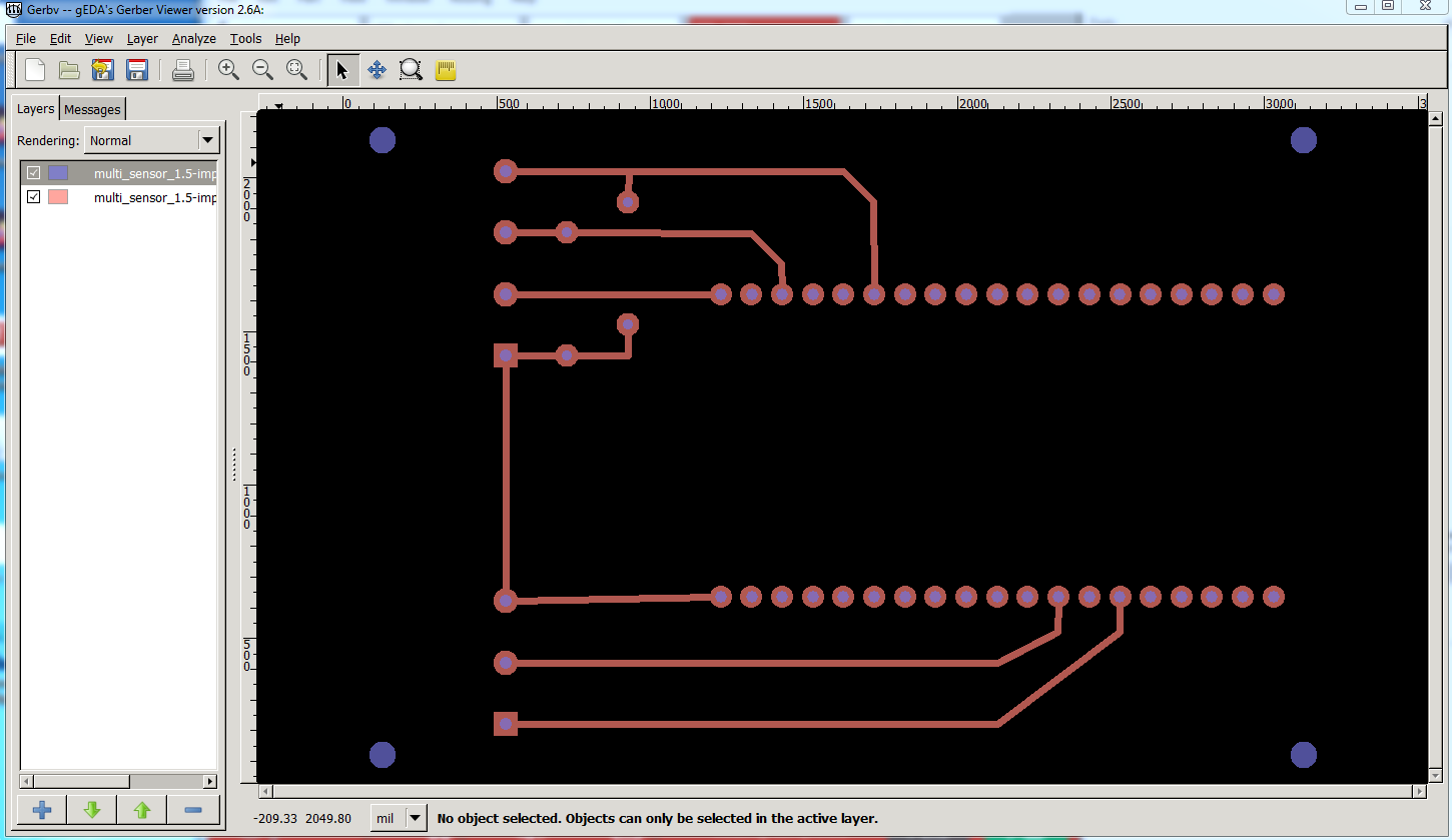
This is the gerbv output from multi_sensor_1.5-improved_drill.txt and one of the copper layers. The purple centers are the drill holes. multi_sensor_1.5-improved_drill.txt looks like this:
T101 are the esp holes, a little large (they should be 0.038in) but close enough to not be a problem. One or another of the esp boards (obviously not this one ) has holes too small for .1 header pins which is why it is wise to check the gerber drill outputs when using parts from the net.
@vanepp I had changed to a different ESP board as I figured out it was not the board I am using. So had to a build of a rebuild. Once I did that - ALL is good.
Now I am resarching who I should actually outsource this to!
There are lots of choices starting with Aisler, who are the fab for Fritzing in Germany. They feed back a portion of their fee to Fritzing development and check the board over before making it. They are fairly expensive compared to the discount pcb makers, but the discount houses don’t check anything and just produce whatever you order. I tend to use elcrow in China https://www.elecrow.com/ and osh park is another that people have used https://oshpark.com/ and liked. There are lots of other choices as well. As before check the gerber drill.txt file to make sure the holes for the esp are close to 0.038 in (the size for .1 header connectors) to avoid the problem of a hole too small.