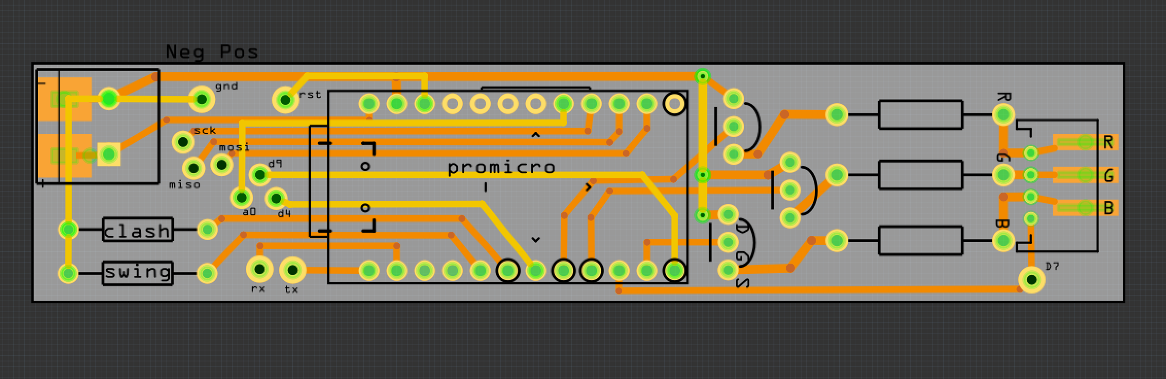
Hi - I’ve just designed this board to hookup an Arduino Pro micro clone and some mosfets and resistors to drive a cree RGB LED in a lightsaber project.
This is the first time I’ve done this, so wondered if anyone had any thoughts on the layout or design before I send it to be printed?
While I don’t see anything fatally wrong here (although our more experienced board folks may ), there are some issues. You look to have used vias (such as rst) for external connection points and they have odd drill sizes. I’d be tempted to replace them with either a single pin header (which has a standard footprint) or possibly a series of connectors unless there is a reason to have them in the pattern that they are. They look to be for external programming and thus an inline series of header pins would make connecting easier. Although it is a connector, on the pcb it is really just a pad and you can connect a wire to it rather than a header if you want. I’d be tempted to actually complete the schematic so you can see that the connections are as you expect as well (and probably breadboard it if you haven’t to make sure it will work). You are using npn transistors rather than mosfets for instance, so you need to insure the leads match up (although from the silk screen notations you look to have done so). You also want to be using logic level drive mosfets, as standard ones typically want more than 5V of gate drive for full conduction. DRC (pcb view routing->design rules check) passes and the gerber output (file->export->for production->gerber looks fine in gerbv (you typically want to check the gerbers with a gerber viewer as that is what the board house will build the board from).
Hey - thanks for the quick reply! That’s all very useful, and much appreciated.
I’ll see if I can rework the connection points and make them into a standard header. It was partly out of laziness because I was having trouble getting a neat layout, and wanted to avoid using the top layer as much as possible. Also, most of those pads broken out probably won’t be needed, but I thought I would break them out in case I did want to use them later on e.g. for extra buttons or sensors. Are there ‘standard’ drill sizes to go for? I think I left it at the default, but increased the ring diameter to make soldering easier…
I have breadboarded the thing (in real life) and it does work. It got a bit cluttered having everything in the single file so deleted the other components, but would it be better practice to have everything in and just drag non-pcb mounted components off the board in PCB view?
One final question… these were the transistors I’d planned on using: http://www.farnell.com/datasheets/528777.pdf I got a bit confused trying to use the built-in mosfet part with the TO92 package size because it didn’t seem to match the datasheet, and this one seemed closer. I think they will physically fit on this board though, and they are logic level as you suggest so am hoping they are suitable…
All the best - and again many thanks for the feedback.
I believe it varies by pcb maker, but they will usually have a list of their drill sizes (the less common ones may incur a tooling charge if used). Some like .035, and .038 (IC leads and .1 header pins in Fritzing) are pretty standard, but you really need to check with the fab house either on their website or by asking them.
That’s what I’d do, because I find in 6 months I won’t remember what I did and why and it is good for the documentation (with the warning that I don’t often make boards I’m usually one of on perfboard)
They look fine (as long as the 100ma drain current is all you need). They are indeed logic level and thus should saturate with 5V drive to the gate. The danger with high threshold gate devices is that they will likely work, but not saturate and thus the device has a high on resistance and replaces some of your series resistor with possibly fatal results (due to over temperature) to the fet. That is one problem with the Fritzing parts (especially transistors) there are so many variations that most are generic and may or may not match your particular pinout. While it is nicer to have a correct schematic representation, creating custom parts can be a pain (although I expect parts editor would let you change pin numbers without a lot of pain) getting a correct pcb footprint with the correct connections is the vital task and you look to have done that.
Hmmm… I think I may have misread the datasheet on that FET. I hadn’t spotted the R(ds-on) was so high.
Would something like this be better?
For context, I’m driving an RGB LED with PWM, where each of 3 channels take .33A at ~3.4V. I don’t expect to drive them at 100% - probably something like 70% max.
Yep this would be a better bet (as long as you don’t mind the smd case). It is always better to have lots of head room in max rating, and the original fet had a 100ma continuous drain current limitation (I did see the high rds on, but with a 220 ohm resistor in series with it, it wasn’t that bad). This one with 1.7A drain current will be loafing at 400 ma which is always a better bet.
 ), there are some issues. You look to have used vias (such as rst) for external connection points and they have odd drill sizes. I’d be tempted to replace them with either a single pin header (which has a standard footprint) or possibly a series of connectors unless there is a reason to have them in the pattern that they are. They look to be for external programming and thus an inline series of header pins would make connecting easier. Although it is a connector, on the pcb it is really just a pad and you can connect a wire to it rather than a header if you want. I’d be tempted to actually complete the schematic so you can see that the connections are as you expect as well (and probably breadboard it if you haven’t to make sure it will work). You are using npn transistors rather than mosfets for instance, so you need to insure the leads match up (although from the silk screen notations you look to have done so). You also want to be using logic level drive mosfets, as standard ones typically want more than 5V of gate drive for full conduction. DRC (pcb view routing->design rules check) passes and the gerber output (file->export->for production->gerber looks fine in gerbv (you typically want to check the gerbers with a gerber viewer as that is what the board house will build the board from).