Hi all…
Have you this part’s .fzp or .fzpz file?
Hi all…
Have you this part’s .fzp or .fzpz file?
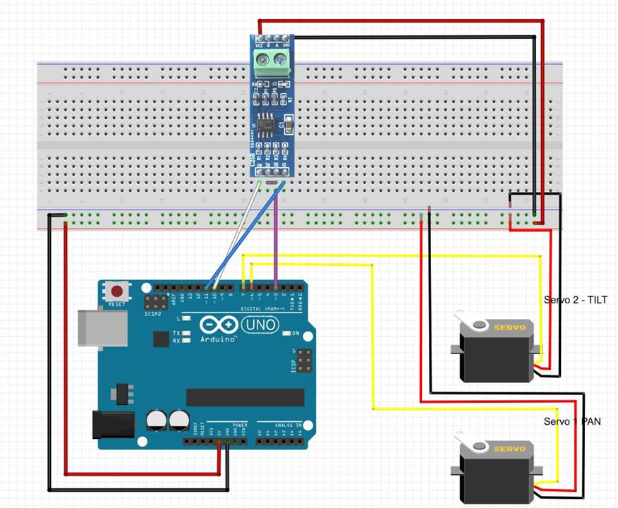
http://constien.info/foren_pics/fritzing_pantilt.jpg
How can i use this part like this picture in fritzing?
Do you have the one for Fritzing?
I have made it!
it is a draft, if it work let me know…
MAX485 Breakout.fzpz (16.3 KB)
At a quick look it seems to have the same issues as your mcp23017 part. If you can’t figure out how to fix then feel free to ask for help.
Peter
![]()
here attached is my last pcb layer…
i spent some times to create pcb layer with dual face but when i import the image on fritzing they return there is was a problem: can not deal with separate copper0 and copper1 layer.
i see your image and use it as master, i don’t know what is wrong! help…
This is the format for groups, silkscreen(part outline) and copper1(top layer), with copper0(bottom layer) inside copper1. Copper0 in copper1 duplicates the pads without having to make 2 identical separate groups.
Simple resistor xml for the svg
https://scontent.fsyd4-1.fna.fbcdn.net/v/t1.0-9/18836073_10211003056686152_3115911194126915049_n.jpg?oh=b57997b35b017ef6d07233a3aab5f877&oe=59A67C29
It looks like your upload didn’t work (if you tried to upload the svg, that is broken in the forums and you need to rename it from pcb.svg to pcb.fzpz then upload the fzpz which does work and tell us that it is really an svg). Starting from the pcb svg in your first upload, in order to create the order Old_Grey specified above (and assuming Inkscape as the editor!) in xml editor select copper0. Now in the object tab on the top tool bar click group. For me that creates a new group in xml editor (called g3625 in my case). Now select that group and in xml editor and change the id to copper1 and set it. Now it should look like the display above with copper1 then copper0 as a group under it and you should be fine. For the silkscreen it looks like the start of it is in g189 and g196 but they are in copper0 rather than silkscreen (and two sides are missing). So select g189 in xml editor and click unindent node twice (which will move that group in to root). Now change the id to silkscreen. Now select g196 and again click unindent node twice to get it in to group root then move it down one position with the down arrow on the xml editor tool bar so it is below the silkscreen group then click the indent node button to move it in to the silkscreen group. At the end of this you should have a group silkscreen with g191 and g196 under it. Now you need to add two more lines to make the other two edges of the board outline on silkscreen (and change the line color to black) and adjust the size of the lines to reflect the size of the actual board outline and pcb should be done. The schematic svg needs to be lined up to the .1 grid and have rectangles added for connectorxterminal on all the pins and you should be away.
Peter
upload was fine, i check again…
if you see my last post on top you see 4 very tiny yellow dots on top of word “here attached”…
click that with right click of mouse and use “save image as” option on your browser.
@Old_grey i try your suggestion, and no error when import, but using the part they not have both layer…
if you can create it, do it! i’ll stay behind if i can’t figure it out. thanks.
Ah! right you are, when I right clicked on the dots I indeed got an svg. Its possible we have been just missing what it does with svg files all this time. Learned something new again! With the svg in hand (or at least in Inkscape) I see copper0 is in the wrong place. g4465 has copper0 under it and copper1 is under g4455 and you have duplicate pads (you only need one set with the proper grouping). To fix it in xml editor click on g4465 and hit delete. That will delete everything under g4465 including copper1 and all the extra circles. Now if you click on g4454 in xml editor and change its Id to copper1 and set you will have the correct copper configuration and it should now work. Your silkscreen looks to be correct now, (if you like you could do an ungroup after selecting g4476 to move silkscreen to root with the coppers, but it should still work as is just fine). With copper0 as a subgroup of copper1 Fritzing knows to copy the connectors to both copper0 and copper1 in the same position so you don’t have to worry about getting both pads properly aligned. You may want to change the stroke:#ffffff in the style command for the silkscreen lines (which is the old standard of white, which doesn’t show up in Inkscape to #000000 (black) which is the new standard and shows up in Inkscape. That should do it.
Peter
It turns out the part above has a problem, in that in pcb it will only connect on the bottom layer due to a configuration error in the pcb svg. Here is a corrected version I made for someone.
MAX485-Breakout.fzpz (12.0 KB)
Peter