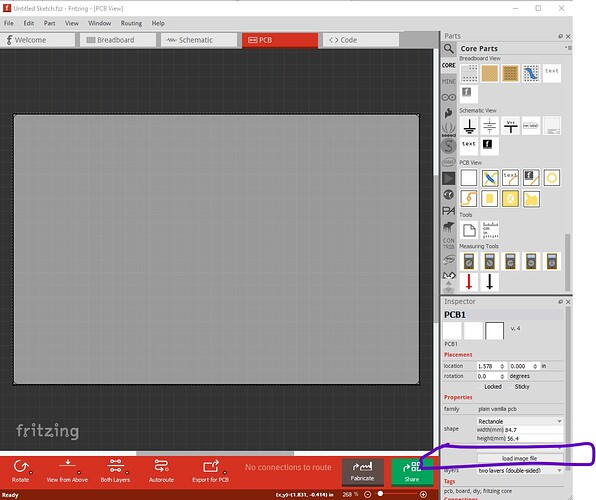
The round pcb is created by loading an image file in pcb view here:
instructions for making the outline svg are here (which uses a circle as an example)
from there things get a bit more exciting. You will likely need a custom part for the bottom part of the board which uses “invisible copper” (copper without a solder mask) to make the outer ring and circle on the bottom layer and plated through holes to the top layer to connect to the transistors and diodes on the top layer. This post discusses blocking solder mask with “invisible copper”
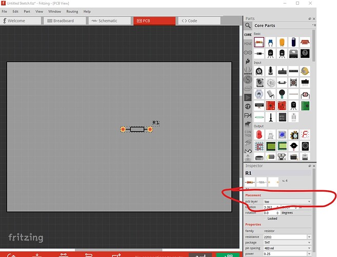
a search in the forum search for invisible copper will turn up a variety of posts about doing this. Basically you will need to make a custom SMD part with the outer and inner copper areas as pads then put that on the bottom layer of your sketch (by changing its position from “top” as shown here on a resistor to “bottom” to move it to the bottom of the board.
Then adding a hole from the pcb section of core parts to the sketch will produce the plated through hole to connect to the pads on the bottom of the board on your new part.
Peter

