Hello Forum,
have only created one rectangular PCB and Aisler produced it in a great way.
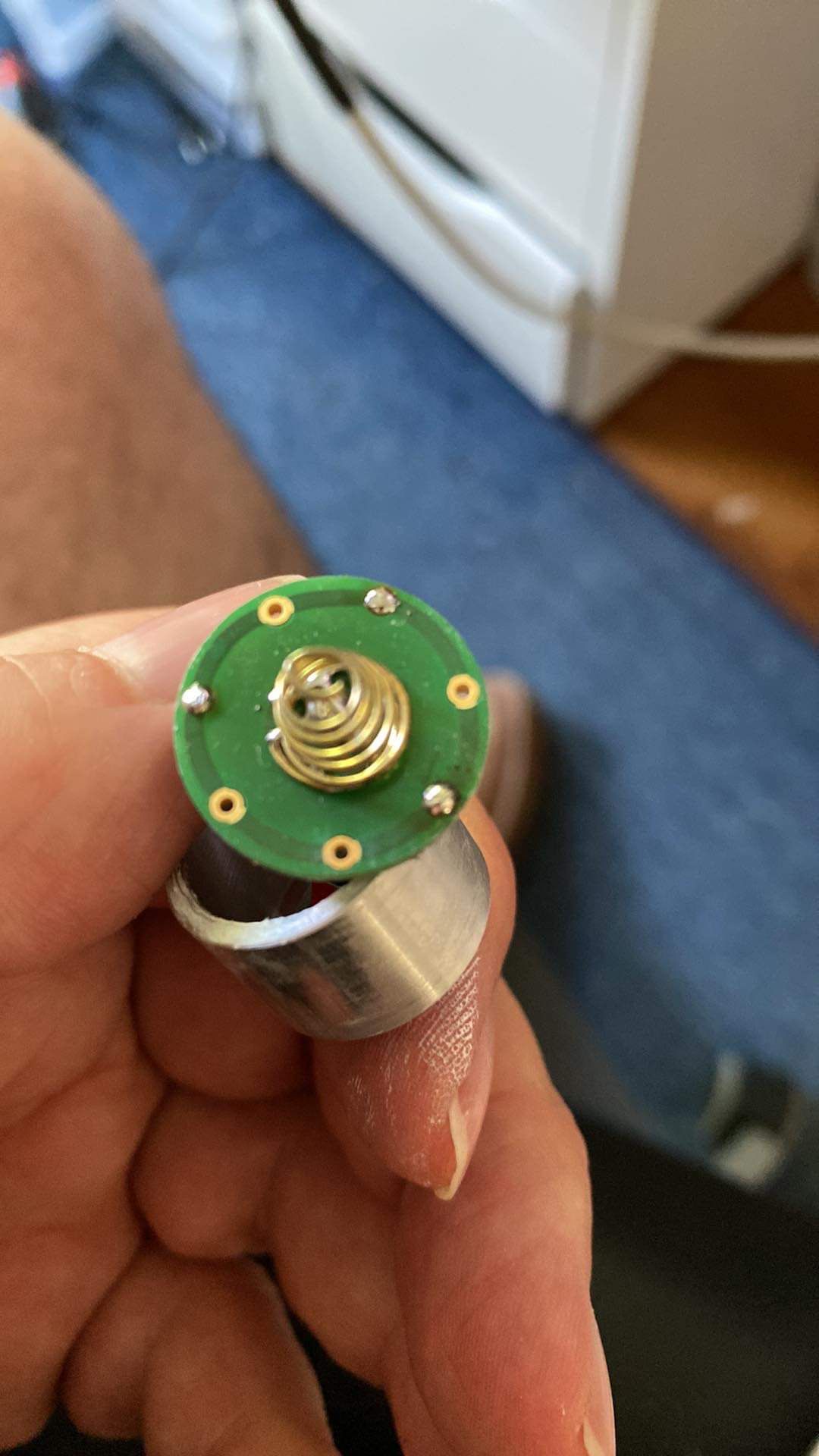
Now I have designed a more difficult round PCB with Fritzing and need to know how I can create a ring shaped solder area and a round solder area in the middle of the 20mm diameter PCB. It is a driver for a LED flashlight.
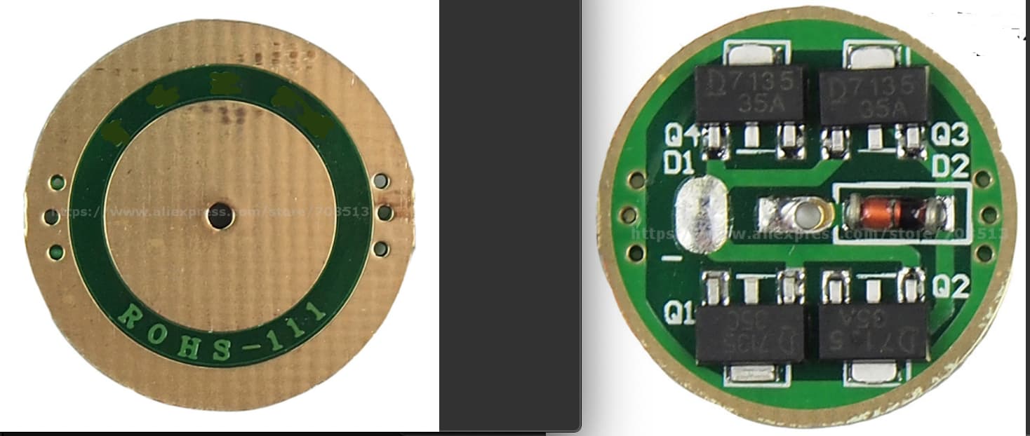
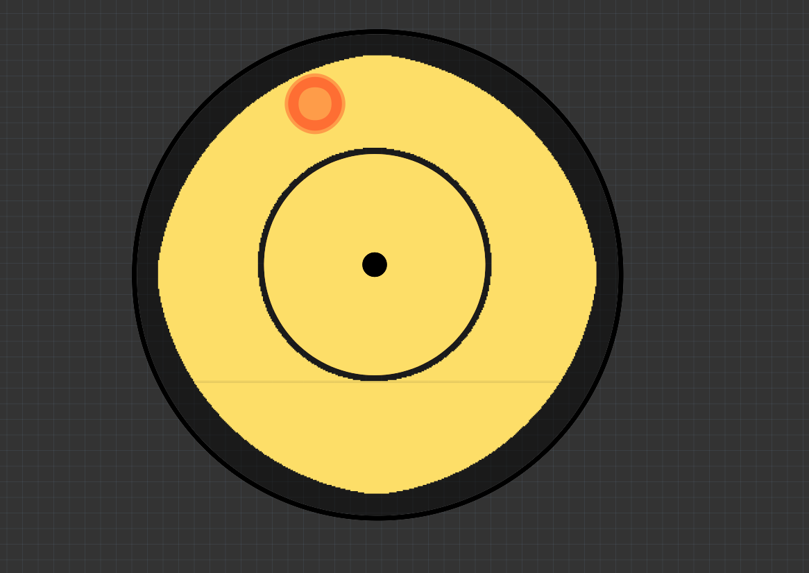
see examples picture from the internet
Thank you in advance
Peter
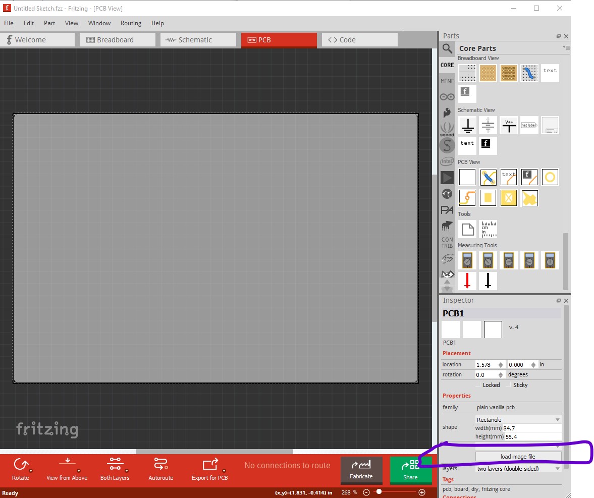
The round pcb is created by loading an image file in pcb view here:
instructions for making the outline svg are here (which uses a circle as an example)
from there things get a bit more exciting. You will likely need a custom part for the bottom part of the board which uses “invisible copper” (copper without a solder mask) to make the outer ring and circle on the bottom layer and plated through holes to the top layer to connect to the transistors and diodes on the top layer. This post discusses blocking solder mask with “invisible copper”
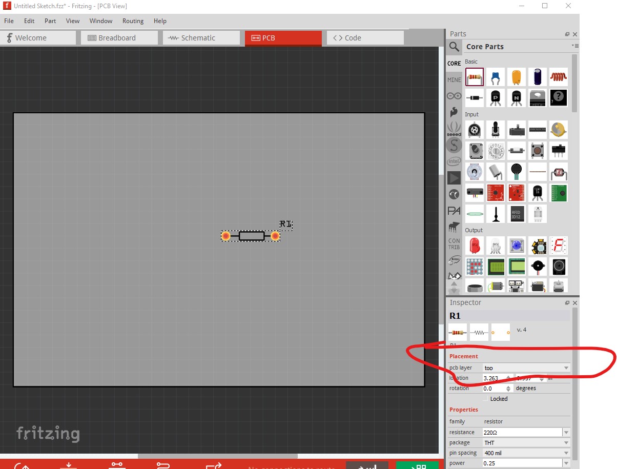
a search in the forum search for invisible copper will turn up a variety of posts about doing this. Basically you will need to make a custom SMD part with the outer and inner copper areas as pads then put that on the bottom layer of your sketch (by changing its position from “top” as shown here on a resistor to “bottom” to move it to the bottom of the board.
Then adding a hole from the pcb section of core parts to the sketch will produce the plated through hole to connect to the pads on the bottom of the board on your new part.
Peter
1 Like
Thank you very much for the quick answer.
Will need to study your answer carefully.
Here is what I am currently have, to show you that I had managed the simple first steps alone 
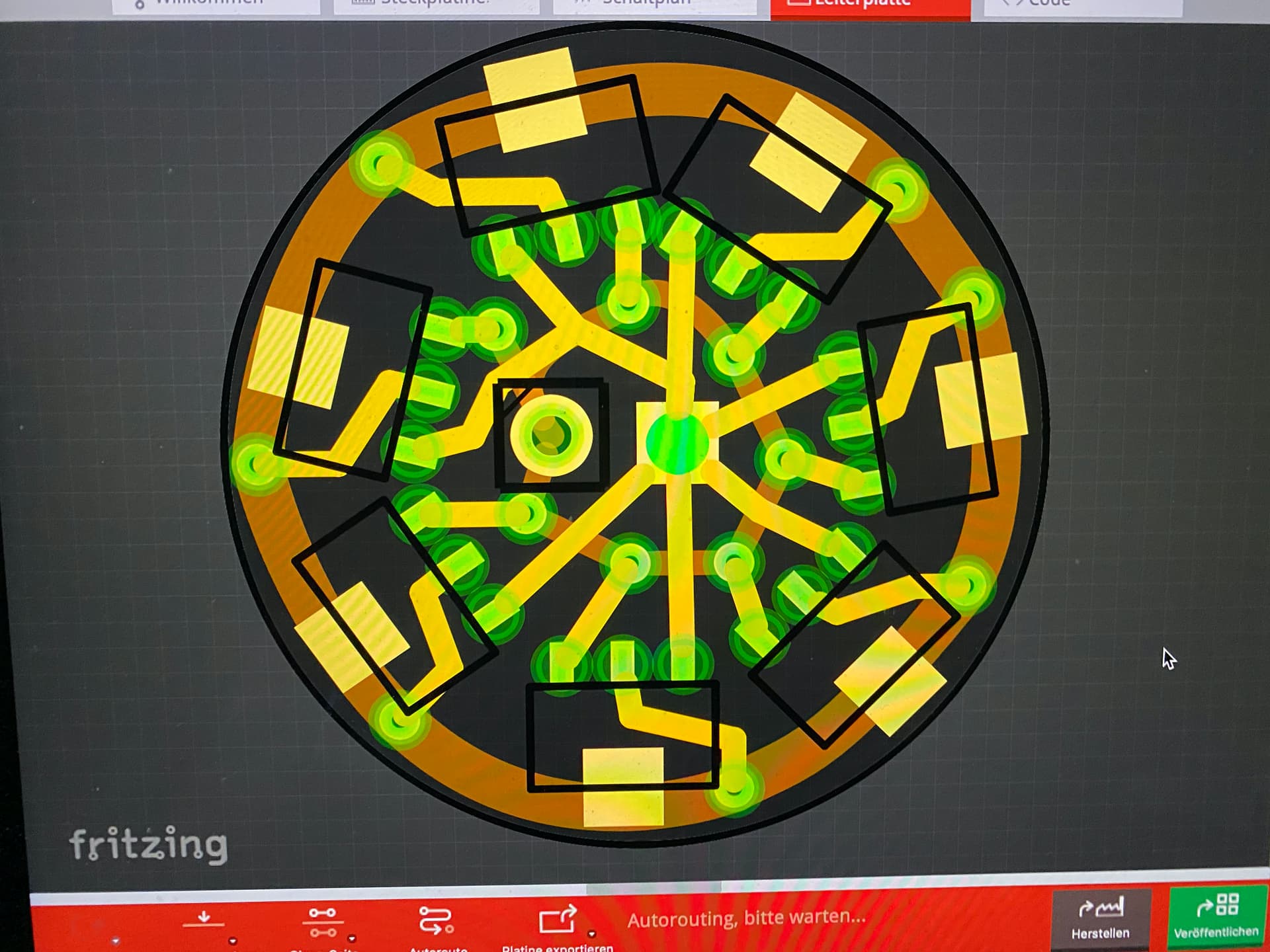
,
1 Like
Hello Peter (vanep),
the invisible copper feels too complicated for me.
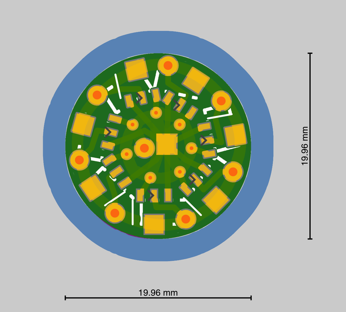
I had tried to use a hole with a ring already and you mentioned that in your answer, so I have tried again in combination with the copper fill.
It looks good, but why are the copper fill not in a good round shape?
Peter, the beginner
PS: No, my idea with the hole/ring and copper fill is not working. 
A screen shot usually does not provide us with enough information about what is being done. The .fzz, .fzpc, or .svg file (depending on the context) provides a lot more information.
It “appears” that svg arcs are beings used, but the centre point or radius are not quite right. Lines are drawn with half of the width on each side of the specifed position. That applies to lines, circle, arcs, and any other ‘line’ based element. So arc and circle radius needs to be reduced by half of the specified width (thickness), to have the outside of the arc or circle match the desired radius. Conversely, increase by half the width to have the inner edge match.
I don’t think it is what you want anyway. It provides board area free of copper and solder mask (which isn’t what you need!) I think your current path is the only one that is likely to be successful, gerber processing appears to fill in the entire inside of the shape ignoring stroke-width. I was intending on using a pad (made of a circle with a stroke width set) which works in Fritzing pcb view but doesn’t in gerber output (as noted the stroke is ignored and the entire circle is filled in. This works for the usual pad because the drill file causes a hole to be drilled in the pad (the gerber copper layer has a completely filled in interior even though the typical pad has a stroke-width and an empty center), in this case we don’t want a hole in the pad just separation between the two pads and it looks like ground fill is the only way to get that. You may have to live with a not completely circular shape unless someone that know more about ground fill than I do has some ideas.
I think the output is from a ground fill of a circular pcb, and thus I don’t think he has much control of the shapes (although I know almost nothing about ground fill as well ![]() ) It may be that a code change will be necessary to get better results, but I agree the next step should be to upload the .fzz sketch file (upload is the 7th icon from the left in the reply menu and will accept the .fzz file of your sketch) so someone familiar with ground fill (not me
) It may be that a code change will be necessary to get better results, but I agree the next step should be to upload the .fzz sketch file (upload is the 7th icon from the left in the reply menu and will accept the .fzz file of your sketch) so someone familiar with ground fill (not me ![]() ) can have a look at it.
) can have a look at it.
Peter
Thank you Peter Vanepp and microMerlin,
for your answers !
I have given up for the time being and ordered my current design at Aisler.
Then I see how it works and improve it when my knowledge is growing.
I am a retired electronic engineer and worked half of my life as an electronic component specialist and the other half as an IT project lead and support specialist.
Now I am learning new things like creating a pcb by my own and not via a big team of pcb specialists.
Have a nice week
Peter
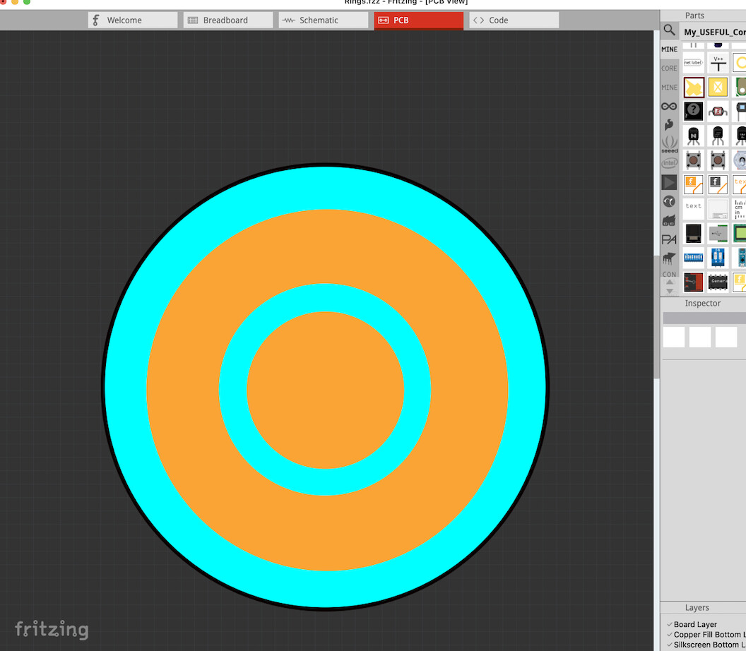
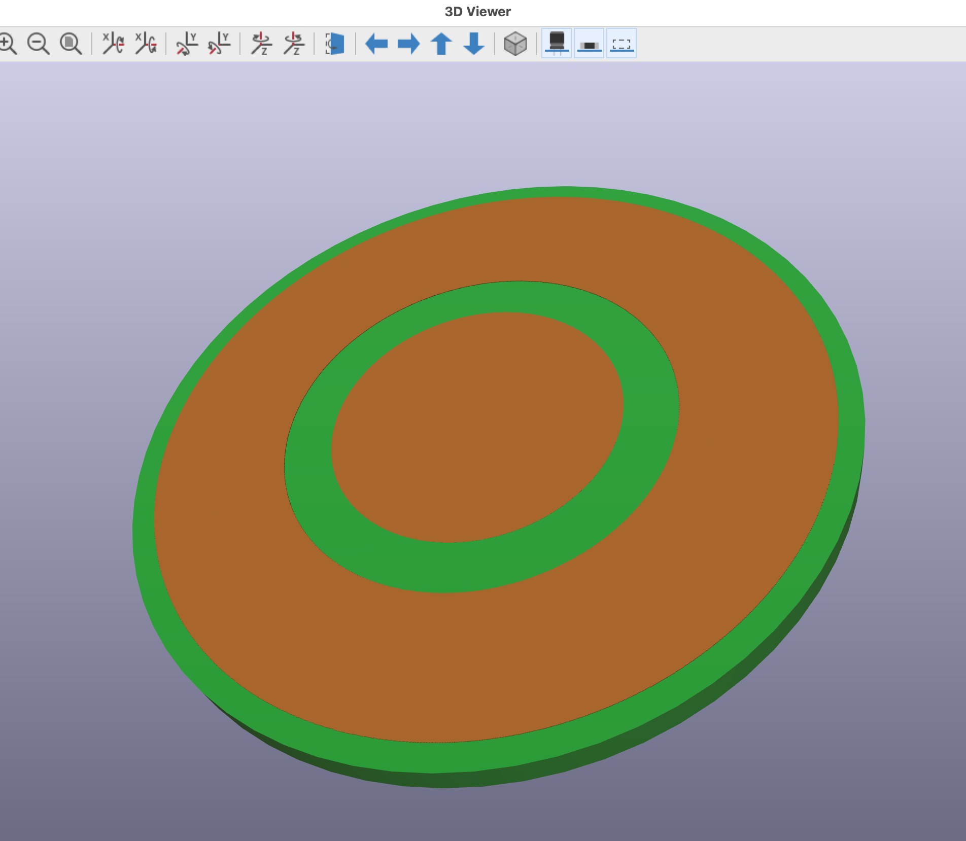
Used Inkscape:
• Draw a Circle for PCB
• Draw larger Ring
• Draw inner Circle for the Gap between the Ring/Circle
• Draw inner Circle a little smaller
• Subtract the inner Circle from Larger (Path, Difference) to get outer Ring
• Save the each as Plain SVG
In Fritzing:
• Load the Circle for the PCB
• Drag Image-Tool-Icon for Copper (I used Bottom). Load the Outer Ring
• Drag Image-Tool-Icon for Copper (I used Bottom). Load the Inner Circle
Now, they are Copper surfaces ready for your parts and traces…
Screenshots of it in Fritzing (and Kicad)

I don’t think this will work. The gerber processing ignores the strokes and fills in the entire circle. Thus when you export for the gerbers (and thus the pcb) the inner circles get filled with copper and the middle ring in the images above gets deleted and replaced with a solid copper pad. It works for pads because the drill layer drills the hole in the solid pad and I don’t think anyone considered any other case.
Peter
Peter
Thank you opera_night and Peter,
meanwhile the PCB has been delivered by Aisler and it worked.
I cannot rate if the proposed solution is working or not.
best regards
Peter O
Looks good… I post the following for other readers…
First: Shame on me!! I haven’t used Fritzing for couple of years and just threw the Round example together.
That said, I looked at some older work and (re)post example, though not using Round images…
All still works well and I just confirmed it using CopperCam to generate Gcode for milling PCB… Without looking into it, I suspect the SVG for the Round PCB was the problem (I did not make it for Fritzing so, it’s missing needed stuff).
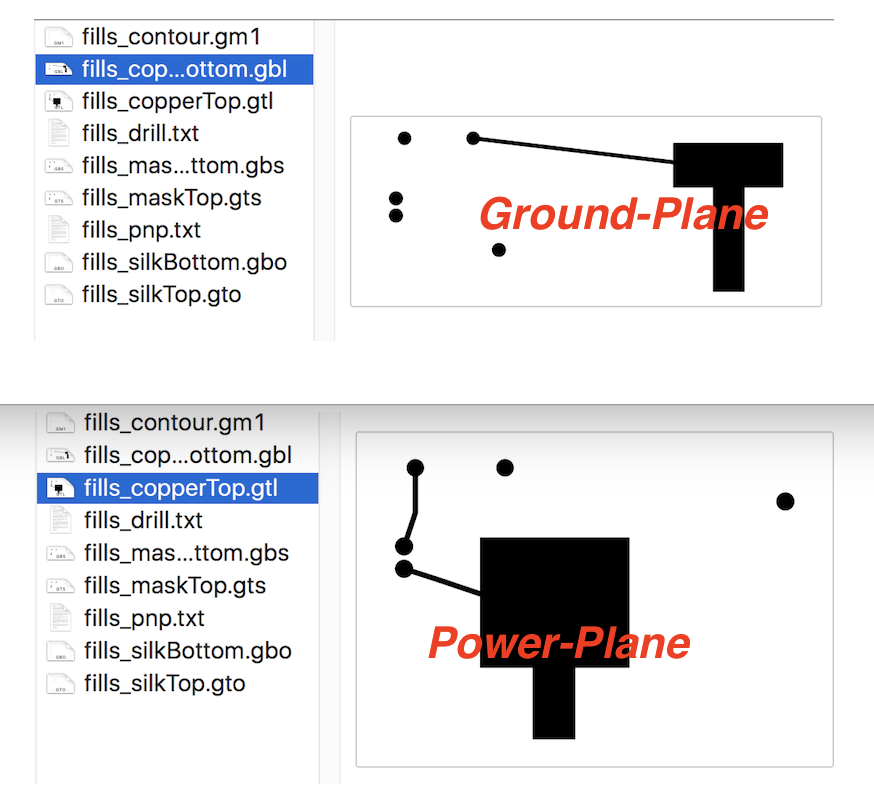
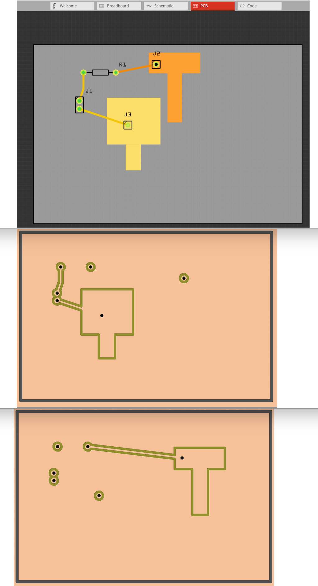
Image of Ground-Plane (SVG). Simple SVG, no layers…