Round board corner issues with Aisler manufacturer

Hello,

I made this new board. But during gerber export it produces 14.000 elements for the rounded shapes. This high number of elements produce some warning when I import the sketch in Aisler website.

I guess Fritzing export draw these arcs as point (I don’t know gerber file format yet).
Are there any tips to avoid that ? Maybe drawing an arc (if it exist in gerber) ?

svg.board.wallmounted_board

If not, I think I’ll review the draw to decompose the arcs into lines…

thanks

FYI…

Though I no longer use Fritzing (preferring Kicad for past few years) this may help:

First - know that various programs that can create shape files for use in Fritzing, usually have Preference panels for setting Export type and things like limiting arc behavior and arc-to-line conversions… (example; FreeCad)

That said:

Regardless of posted info and documentation indicating Fritzing needs Layers defined in the file, they really don’t. You can create a PCB svg file by just drawing the shape and saving/exporting the SVG. I’ve done that with a handful of drawing programs.

I just now did this to confirm my poor Fritzing-user memory.

In fact, here’s what I just did to confirm Happiness!

Created a PCB Shape in FreeCad (no layers, did nothing beyond draw it) and Extruded it to fill-in the shape as a solid.
Exported it as Flattened SVG.
The SVG file size is 3kb (very small)

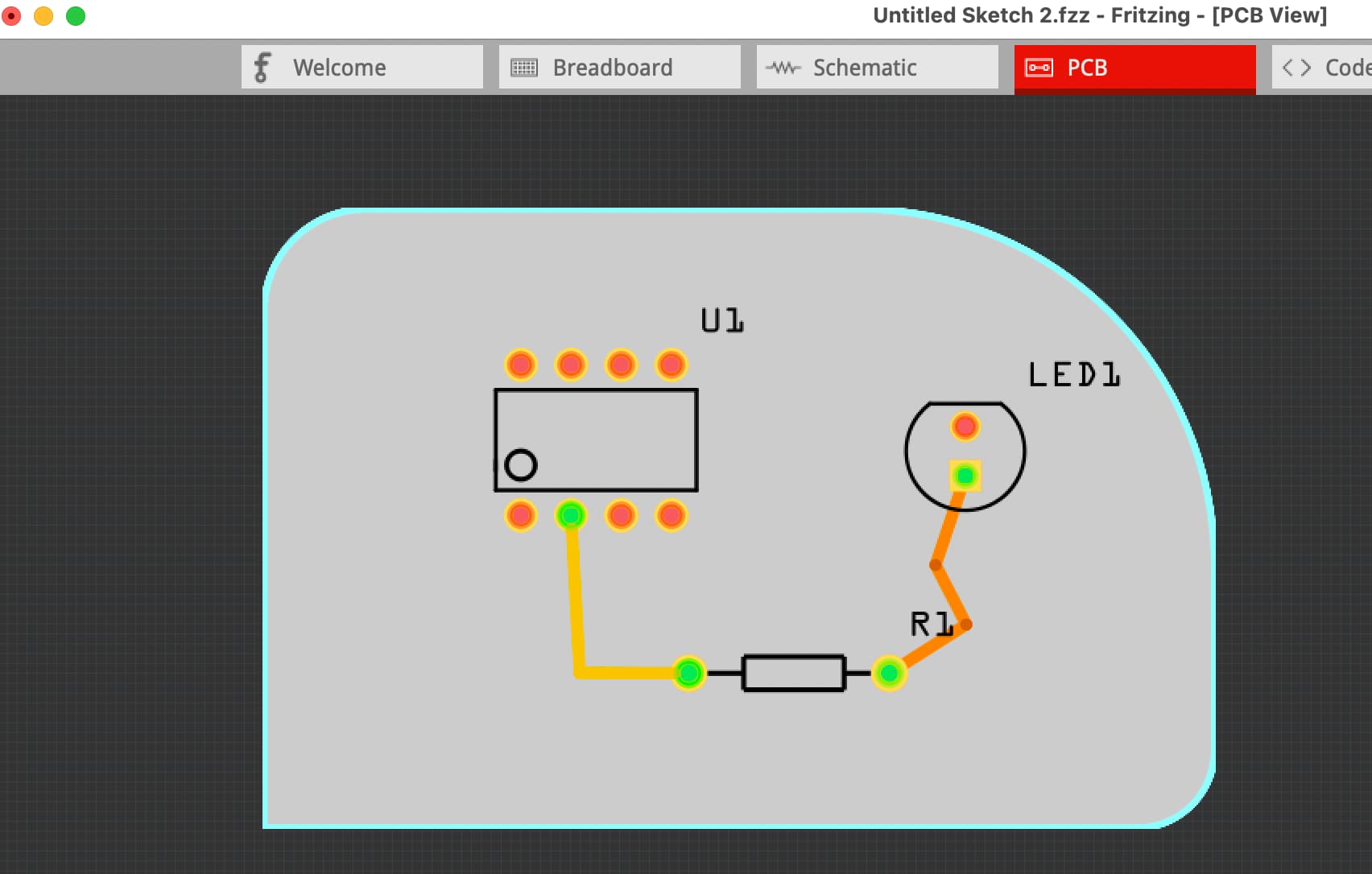
In Fritzing (my old version) I loaded the PCB shape and added a couple of Parts to it and added Tracks to Top & Btm

Then, Exported Gerber’s for Production.
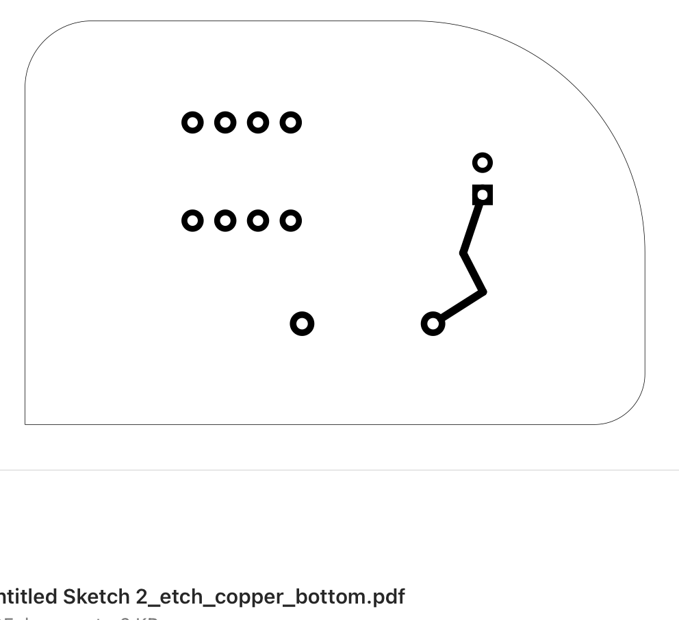
Also, Exported to PDF

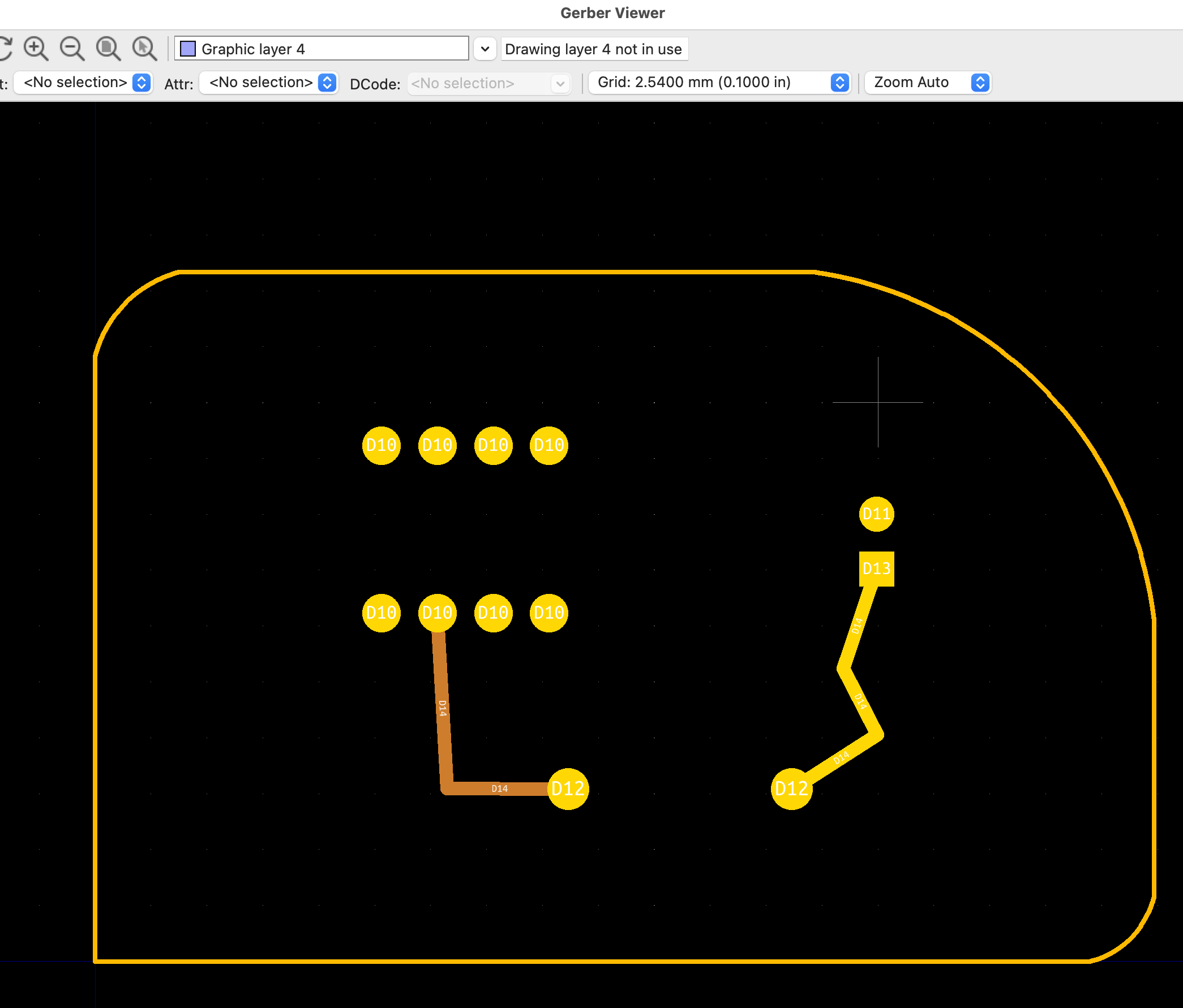
Then, with GerbView (Kicad’s Gerber viewer), I opened the Gerbers. No problem.

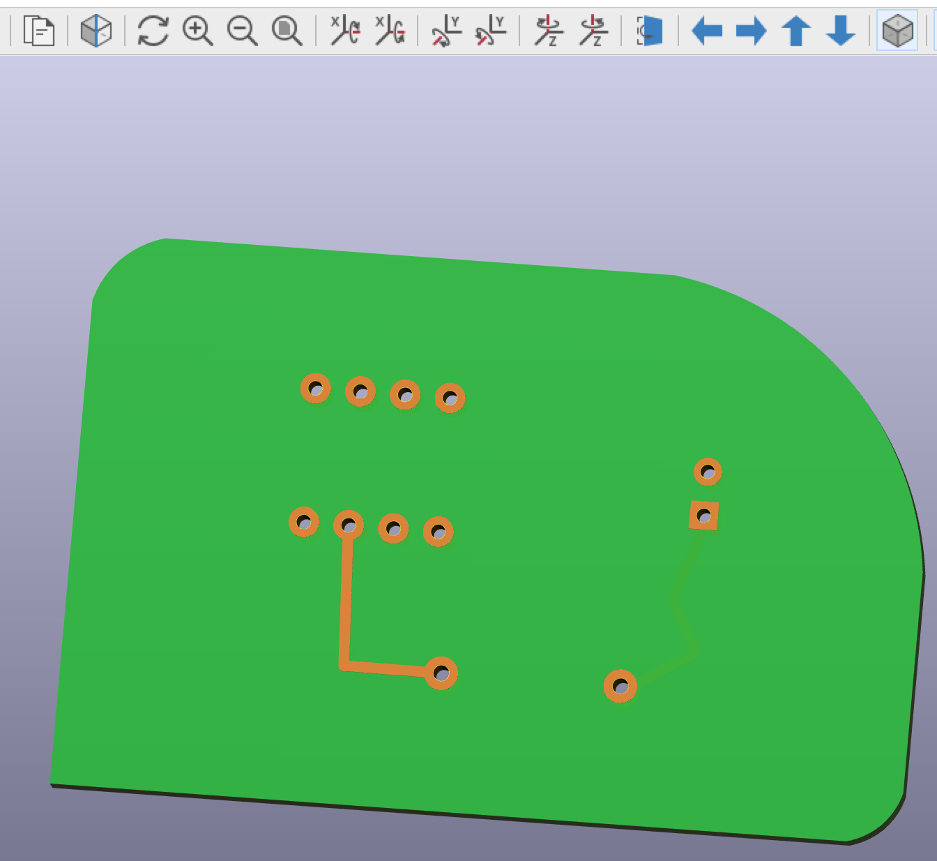
Then, I exported-to-PCB (a feature in GerbView)

Then, I opened the exported PCB and moved the PCB’s shape to the Edge-Cuts layer (that’s where Kicad wants the shape). No problem

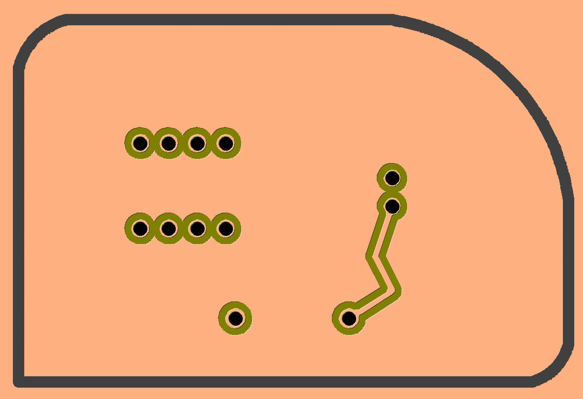
Some screenshots… Mostly to show/confirmation…

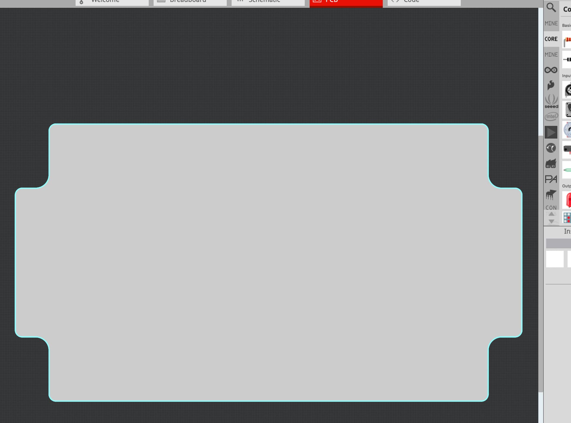
PCB Loaded Into Fritzing
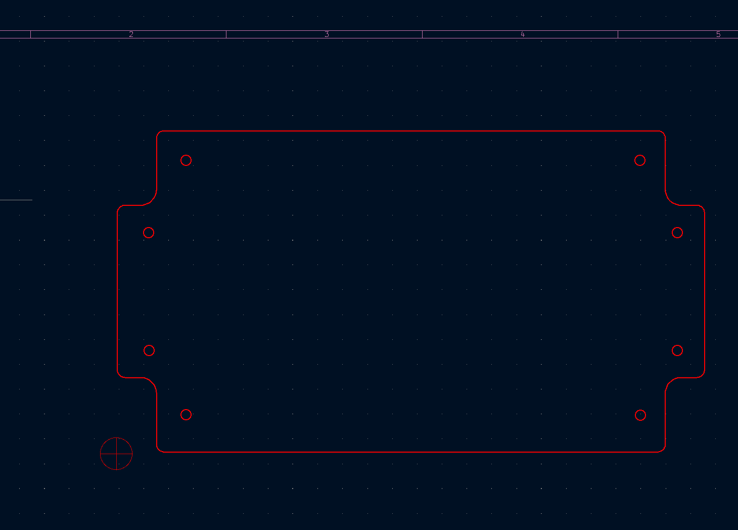
In GerbView

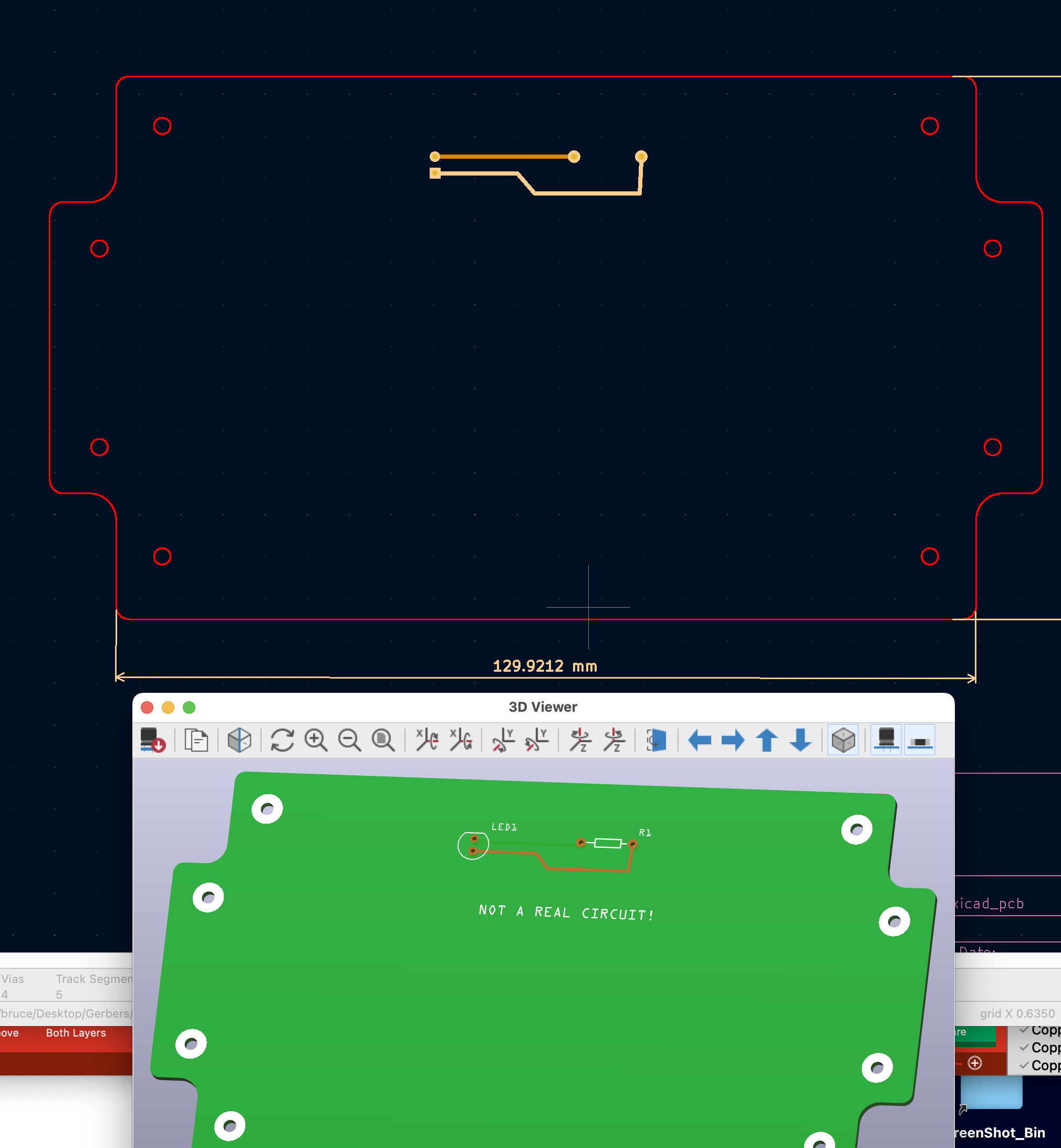
In Kicad, Moved Shape To Edge_Cut Layer
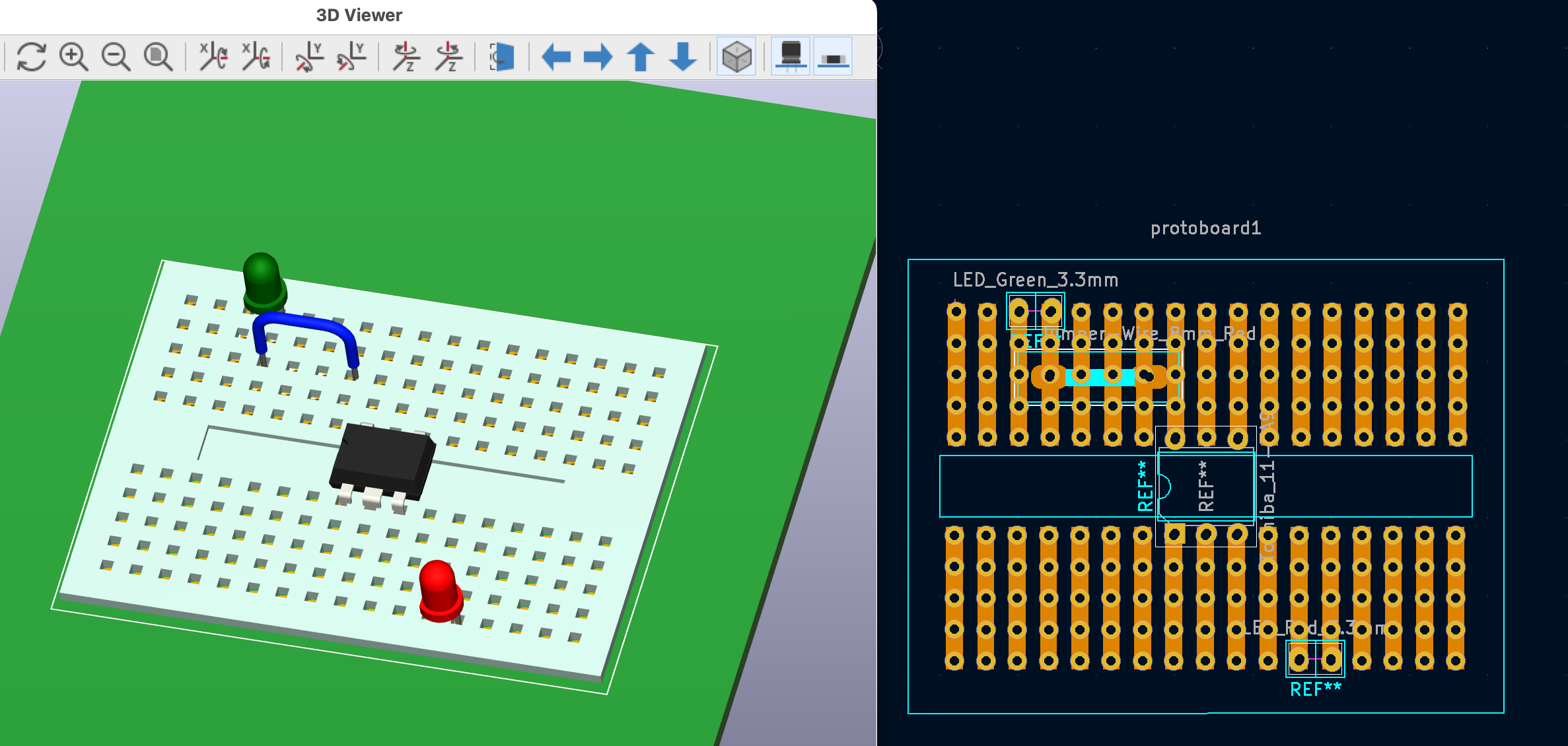
Kicad’s 3D-Viewer…

PDF of Copper_Btm (small 2kb)
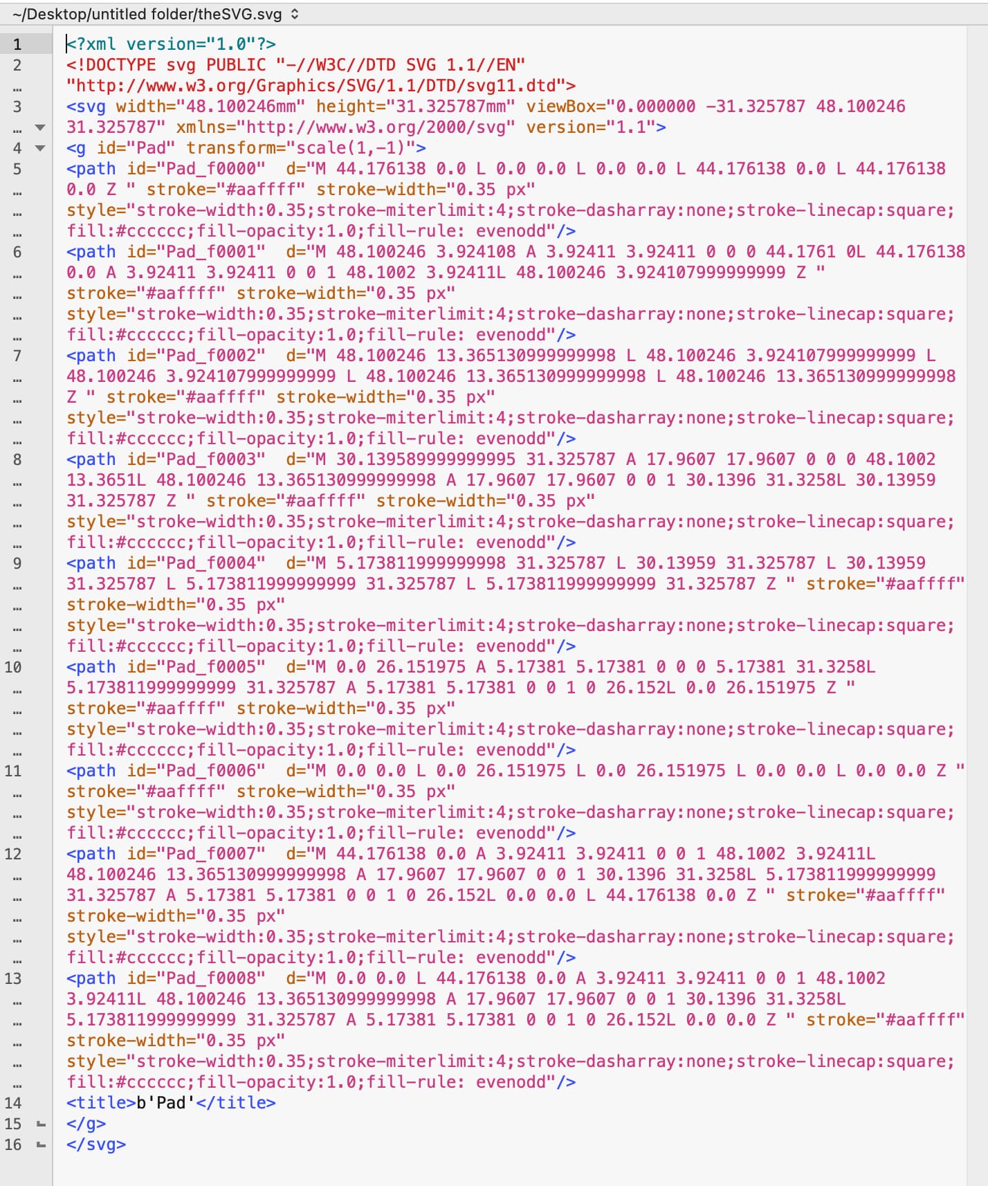
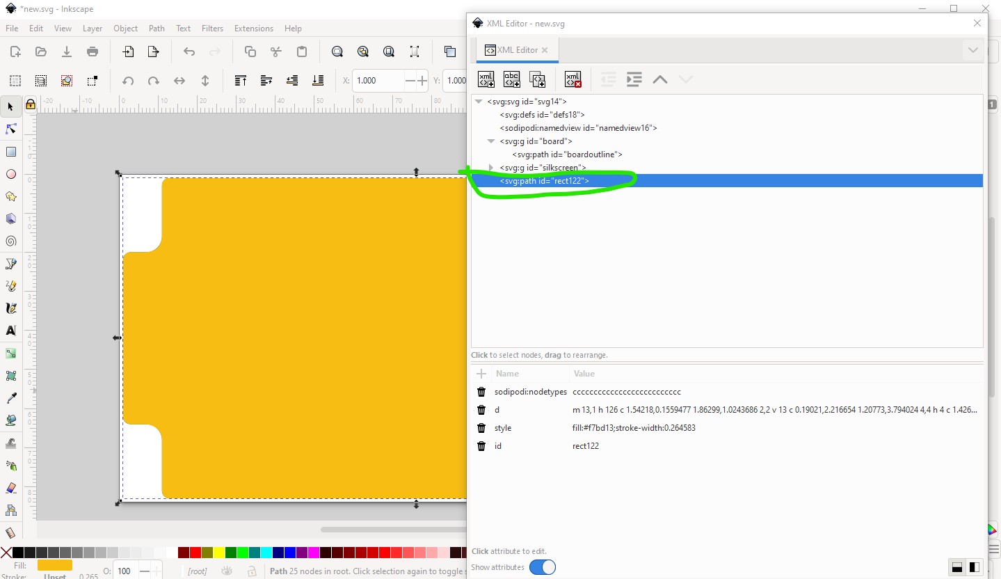
The SVG
theSVG

Screenshot of theSVG (to confirm Not creating Layers…)

For Fun, I loaded the Gerbers into CopperCAM (the program I use for CNC Milling PCB’s)
I did NOT setup any parameters (that would be needed for actual machining (tool bits, drill diameters…etc)). Just did it to do a Full Confirmation…

As you can see, All works Well! :grinning:

thanks for the feedback.

As I’m nto good at all with freecad and kicad, could you attach a square board with only one curved corner in both svg format (svg file) and gerber format (contour.gm1) ?

Or convert mine as a gerber file with these tools ? (the easiest for you, it’s for a diagnostic)
thanks

Sure… BUT, you have to Answer the Question Marks ( ? ) in the attached and, specify PCB board thickness (typical value is 1.6mm +/-…) and, may as well specify a Color…

Also, if you want to do some learning… here’s a link to my vid I posted yesterday (for a Kicad user) but it will apply to Fritzing PCB shape, too, just export Flattened SVG instead of DXF…

Ooops… Forgot: Before Exporting the SVG, you’ll need to Extrude it (called ‘Padding’ in FreeCad). Perhaps confusing at this Noob juncture but, you can do it with One-Click in either Part-Design or Part workbench’s. If you post your Shape, I’ll look at doing it…

Example - You decide which corners to Radius…
fillintheblanks

Here is a copy of your outline (I don’t know how to make the interior holes in the path editor in Inkscape)

it is overlaid on your original path but looks quite different (Bézier Curves rather than arcs) and is how I usually do these. To me it looks like your original one should work, it displays correctly in gerbv. The interior holes are made from 2 arcs, but that appears to be normal from what I can see.

new

Peter

@vanepp Seeing your posted image (of pcb) made me look at the OP’s posted image. When I didn’t see an SVG File or any file posted, I figured you used the browsers xml.

That prompted me to remember I could get the actual, usable image xml data with two clicks! Bingo!

Having done that, I’ll first comment re below):

SVG’s have an ‘Intrinsic Subtraction’ (like ‘Difference’ manipulation). It works by Drawing the shape ‘Counter Clockwise’ assuming the parent container was drawn ‘Clockwise’. Commonly referred to as the 'Fill Rule’s ‘nonzero rule’.
See Painting: Filling, Stroking and Marker Symbols — SVG 2

And, of course in Inkscape and most other’s, you’ll find a Menu-Item in one of menu that shows: 'Difference, Subtraction, … [you select the Parent and the Hole/others and Click! No xml code to mess with (you just forgot about that stuff…)

Back to the PCB

  1. I grabbed the posted image’s xml and pasted it into text file (UTF-8 font). [I use BBedit for this kind of stuff but, any editor works].
    I saved it with .svg extension

  2. In Fritzing, I loaded the file into the PCB and added some parts and silk-layer text

  3. I exported Gerbers and PDF

All aspects worked Perfect (and, I’m using v9.3 ).

Confirming all worked well, I did this:

  1. Opened the Gerbers in GerbView, Exported To Kicad_PCB

  2. Opened the Gerbers in CopperCam

  3. Opened the SVG in FreeCAD

Again, all aspects worked Perfect And, all file sizes were in kb, no Meg size files,

Dimensionally, the PCB may be different than user intended - Got to consider DPI, Display…etc.

Fritzing file and Some screenshots…
toFritz.fzz (3.3 KB)

[I couldn’t figure out how to upload the file - download shows up as this Image]

svg.board.wallmounted_board

As Opened in Fritzing with some Rulers added for ref.

Exported Gerbers from Fritzing to GerbView (I didn’t bother changing silk around holes)

Nope, if you right click on the image in the first post and select “save image as” it will download the svg. The forum has been fixed to properly display the svgs now (and thus be able to save them with a right click.) I’m guessing the problem is that the gerber contour.gm1 file has 13,831 lines that looks like this

G04 MADE WITH FRITZING*
G04 WWW.FRITZING.ORG*
G04 DOUBLE SIDED*
G04 HOLES PLATED*
G04 CONTOUR ON CENTER OF CONTOUR VECTOR*
%ASAXBY*%
%FSLAX23Y23*%
%MOIN*%
%OFA0B0*%
%SFA1.0B1.0*%
%ADD10C,0.008*%
%LNCONTOUR*%
G90*
G70*
G54D10*
X707Y3022D02*
X708Y3022D01*
X709Y3022D01*
X710Y3021D01*
X711Y3021D01*
X712Y3021D01*
X713Y3021D01*
X714Y3021D01*

X506Y3267D01*
X507Y3268D01*
D02*
G04 End of contour*
M02*

where the bulk of the lines appear to be dots spaced probably 1/1000 of an inch apart given x and y are increasing 0.001in per line (if I am reading this right.) I don’t know gerber format nor what a normal contour.gm1 file looks like. The only file I have that I know was successfully made in to a board by Aisler is a triangle with a triangular hole in the middle and its contour.gm1 file is only 438 bytes long (but also has no curves.) As to the internal holes in the path editor, I don’t know how to create a node in the middle of the path (only how to make one on the edge) so I can’t create the nodes for the holes. I could undoubtedly read the Inkscape docs to figure out how, but I don’t usually make such paths.

Peter

I’m always humbled by my stupidity!

Yes, the Gerber has many data points.

Yes, I understand how to open the Posted SVG’s (your post reminded me).

So, I reread original post text - slap me in the head! The problem isn’t with SVG, perse’ or Gerber. It’s with how Fritzing makes the Gerber (Nope!.. keep reading…)

No Curves = minimal data points

Yes Curves = many data points

But, the real problem is with Aisler. I’ve been spending past 3yrs on Kicad Forum and many folks have similar problems (and more) with Aisler files…

Kicad has Zero problems loading Gerbers from Fritzing for this PCB.

I also loaded Gerber for PCB with and without Radiused corners: Those without Radius are minimal lines of data. Those with Radiusd have many lines of data.

Therefore, it’s Aisler not happy with larger gerbers. One Caviot: If user is using a Free or Trial version (of most software’s) there’s often a limit on how much the particular app will do until unlocking the license… worth asking/checking…

He is using Fritzing (don’t know what version though) so no limits there, so I expect the issue may be with Aisler either with thier viewer complaining when there isn’t a problem or with their viewer (or possibly later software which can’t deal with large contour files. I think people have gotten boards with curved outlines (I have debugged a number for people) but I don’t know if any of them used Aisler or not (or really, if they got working boards) other than the triangle case which is no curves. I expect the best bet is to ask the Aisler support folks if the original svg is really a problem, they are likely (other than taking your chances and ordering a board and see what comes out!) the only ones that can give a dependable answer, I certainly can’t other than to say the output looks correct to me in gerbv.

Peter

Thanks for your contributions.

I dug a bit more into this arcs situation. Fritzing rasterize curve and plot them as a tiny short segments of maybe 1/100inch (as @vanepp mentioned) into gerber files.
@opera_night I tried with Kicad, which seems to use arc commands (I-xxxxJ0 command I think)

As far as I understand the purpose of Gerber, each line is an order to the robot to cut, to drill, … Producing 14000 commands is maybe a bit intense for a robot, probably as much as printing 14.000 segments next to each other to draw a line on a printer/plotter, while they may have optimized algorithm to smoothly and quickly move along an arc.
So I don’t mind and made myself a reason that a manufacturer raises warnings for that.

I guess I’ll play with cosinus and sinus to change my arcs to few short segments.

Aisler confirmed that long list of small moves with a very small milling tool implies to use a non classical robot (more expensive).

I made a little program to help transforming arc to a list of straight lines.
The board is well imported, but I didn’t pay attention, in the all list of warnings, to the holes. They are also part of the problem. That would worth to push a bit a enhancement of the gerber export feature.

I guess I’ll remove holes from the board and put them in fritzing (removes advantage of having a board)

svg.board.wallmounted_board.line8

This exercise was well worth doing for me - Why? Keep reading…

• I loaded the original shape (svg) in FreeCad and discovered all the curves were made from Bizers. Thus, between the curves and holes, a ton of data results in Gerber.

• I re-drew the shape using Lines and Fillets and Circles - Did NOT use Bizers.
Exported DXF and SVG

• I imported the DXF into Kicad and exported Gerber of shape with the Holes.
The Gerber file is 3k and has 141 text lines in the file. Very Small

• I imported the SVG into Kicad and it did not like the corner radius or holes. I could have tweaked this in Inkscape but didn’t bother

• I imported the SVG (without Holes) into Fritzing and exported Gerber of shape without holes (could have added Fritzing’s ‘Hole’ parts but didn’t bother.
The Fritzing Gerber has zillions of lines and file size is 167 kb, large file compared to Kicad’s Gerber (which includes the Holes).

So, Summary:
While Fritzing has some nice features/aspects, I am so glad I switched to Kicad. It was easy enough to learn and is far more powerful and capable than Fritzing (sorry Fritzing folks, I too was a fan until after switching to Kicad).

It’s not clear to me ‘Why’ user wants to use Aisler by loading Gerber’s into it - Gerber’s are the final Output for making PCB - he already has them.

I leave it here…

Screenshots

Kicad’s Gerber - Snippet (couldn’t screenshot all 141 lines)

DXF loaded into Kicad

SVG loaded into Fritzing

You would need to make an enhancement request on qithub (pointing out Aisler has an issue with the current output may help that!) There was a major rewrite of the gerber code (some 6000 commits) in progress about 5 years ago (probably done longer ago than that) which got tried (before development restarted) but had to be backed out because it had too many bugs in the gerber code. It will still be in the code base as a branch I expect so that may be somewhere to start from. The original authors didn’t respond to email when some of us tried to fix it and the project was abandoned (and most of the people involved no longer post here …)

Peter

That is entirely true, as long as you are doing boards. Breadboard is the reason I stay with Fritzing which AFAIK only tinkerbox (whose disadvantage is closed source cloud based so if AutoDesk shuts it down you are out of luck) has breadboard view. These days I rarely make boards just wire prebuilt modules together so breadboard view to document them suits me. Depends on what you need to do. Someone was (possibly still is, it was a large project!) working on adding ICs to reverse engineer existing pcbs back (which have apparently been lost to time) to schematics to make updates. Fritzing was the only thing he found that would go from pcb to schematic. So there are use cases where Fritzing is useful even with its limitations (and development is fixing some of those!)

Peter

I understand. In fact (and, I’m Not hoping to sway folks away from Fritzing) when I came to Kicad from Fritzing (fyi - I came to Fritzing from Eagle and PCB123), I missed the BreadBoard aspect as I often prototype on BreadBoards.

Because I missed the BB ability, I jimmied-up a way to get BB in Kicad. Sure, it’s not as nifty as Fritzing’s BB but…

Basically: I created a PCB with THT/pads and Created a Footprint. Also, I created 3D-Models of BB.
(Kicad calls Parts for the PCB, “Footprints” and calls parts for the Schematic, “Symbols”. User can link them together for efficient/flexible use).

So, I linked the 3D-model to both a Symbol and a Footprint.
I set the Height of BB-model to be above the PCB and made the BB-model thin enough so component Legs, Pins, etc poke through the BB and contact the PCB.

Works Perfect! (sans the nifty stuff Fritzing can do with BB and parts/wires).

Making Footprints is simple (much faster than making Fritzing parts and custom board…)

I sorta miss using Fritzing but I’ll stay with Kicad (never know when I’ll need multi-layer PCB’s) And, I really like CAD work so, making 3D-models and Footprints are fun/easy for me and, quick!

Plus: Kicad has embedded NGspice and I managed to link LTspice to it so, I can go either way for simulations :grinning:

Screenshots

Already “requested”, I read aisler is great Fritzing supporters.

KiCAD is probably great or super great, but it’s a bit raw not user friendly. Something I like about Fritzing is I can make part or boards and be sure at 100% of their dimensions, because I can write the svg file without graphical tools (it’s unusual, I know). This save me some money and avoid waste of boards…

Stephane