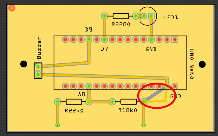
I’m trying to modify the path of the gray line circled in red to match the yellow conductor at an angle. Thank you for your help.
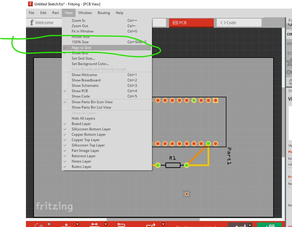
When requesting help always up[load the sketch to the forum so we can see the actual sketch you are having problems with (the sketch is the .fzz file and upload is 7th icon from the left in the reply menu.) First click on the view→align to grid tab to enable snap to grid which will cause the traces to align to the 0.1in boundaries (you will need to move all the components to snap them to the grid for this to work though.)
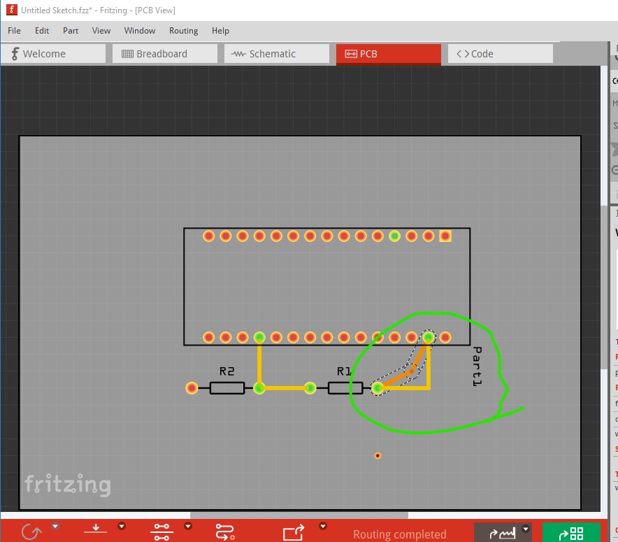
Then to move the trace, click in the middle of it and drag it in the direction you want it in the direction you want it to go (the bend point will snap to the grid!) like this:
Note it is not sensible to have two connections to the same pin as that is likely to cause a ground loop though.
Peter
1 Like
Alarme 1couche NANO 15-12-2025.fzz (25.2 KB)
Here is the file not modified. Thanks for your help.
You have a number of problems. Your ground fill is not appearing correctly in the gerber output, likely meaning that the ground fill set up is incorrect or that there is a bug in Fritzing.
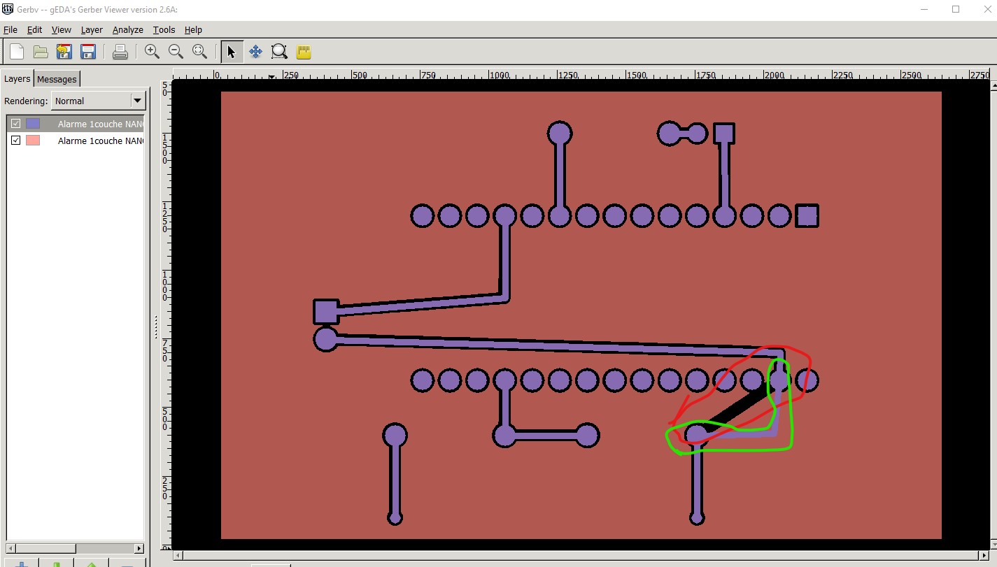
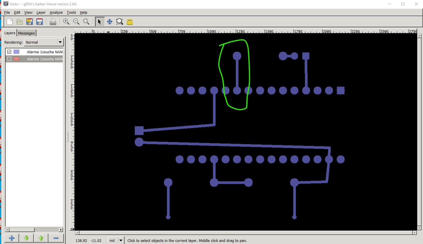
The diagonal line circled in red here should follow the trace in green. As this stands it will work as the ground pin is connected to the copper fill, but it is not correct. The second problem has nothing to do with ground fill, You appear to have connected the same pins on both the top and bottom copper layers. This is incorrect. The connection should be on either the top or the bottom layer not both. Connecting both may cause ground loops as there are two paths to the same connection and is a bad practice. This is the bottom layer in the gerber output with one trace outlined in green.
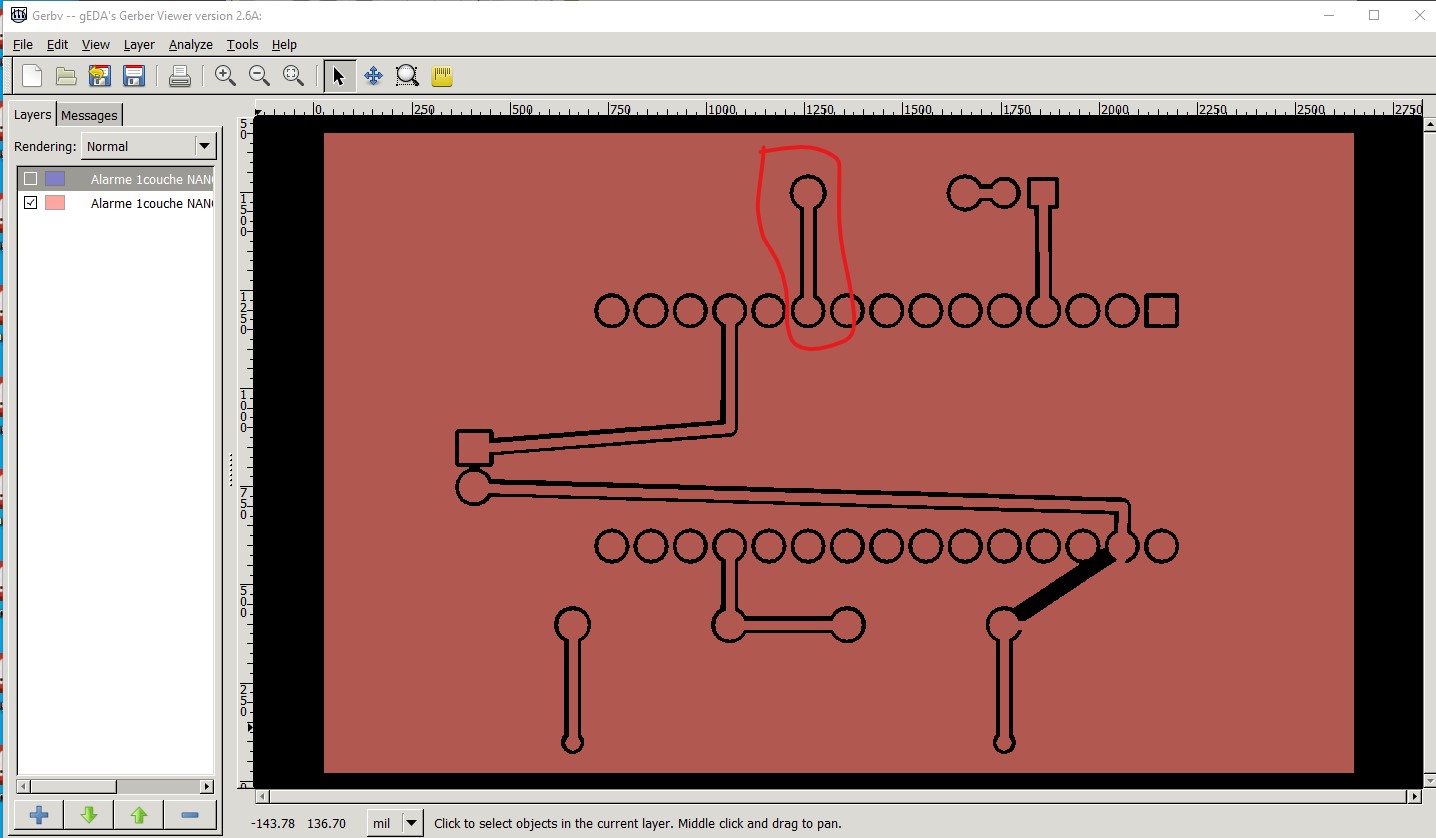
This is the top layer with the identical trace also on the top layer which is incorrect circled in red. You need to eliminate either the top or bottom trace in each case..
Peter