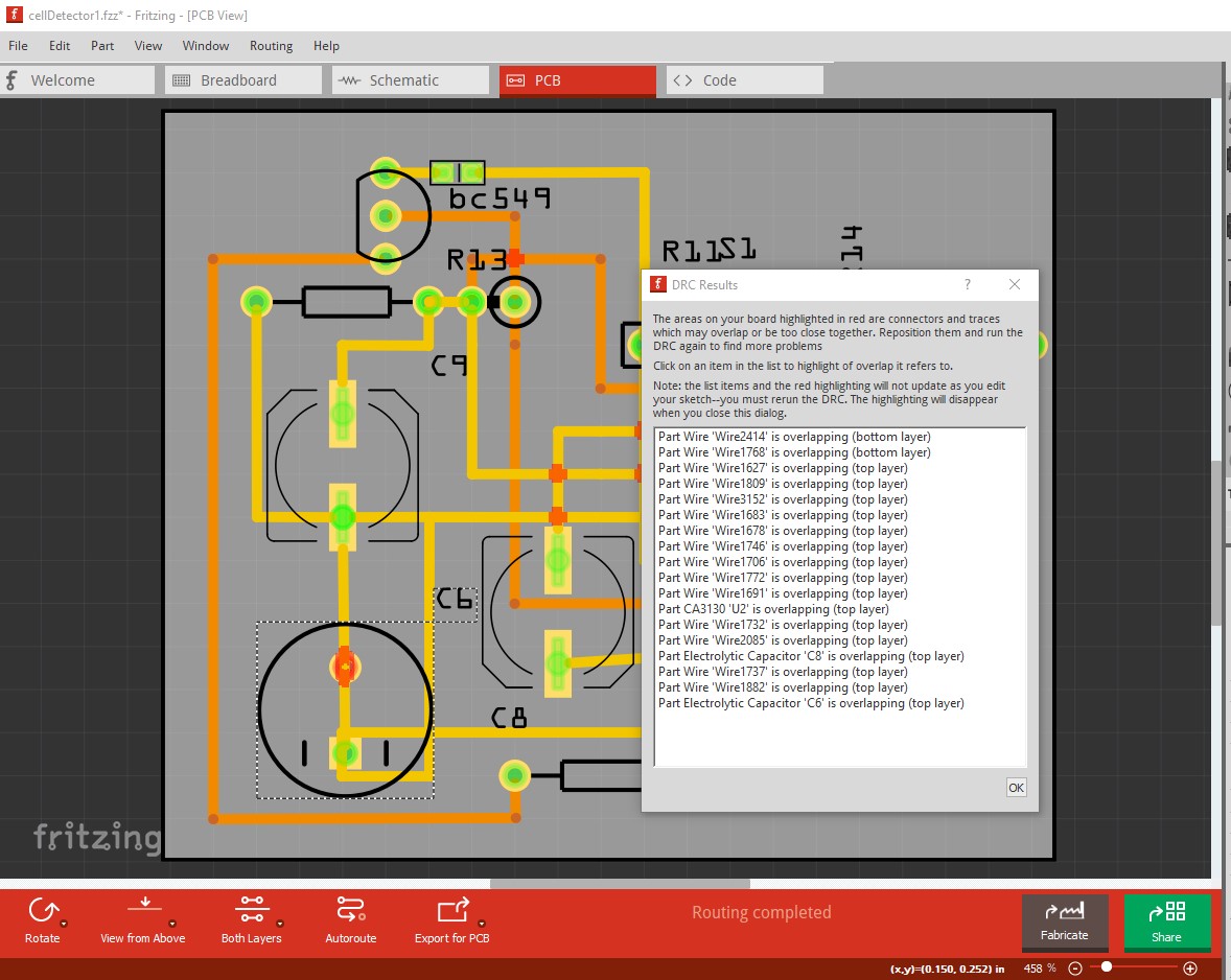
Hi, if somebody has time could they please check my circuit project of a mobile signal detector, I’m following this YouTube tutorial, I have attempted my interpretation of the circuit for a manufactured pcb project but am new to Fritzing and am unsure if I have the circuit correctly created. My project is added for easy collaboration if somebody wouldn’t mind looking it over for mistakes, thank you. cellDetector1.fzz (27.4 KB)
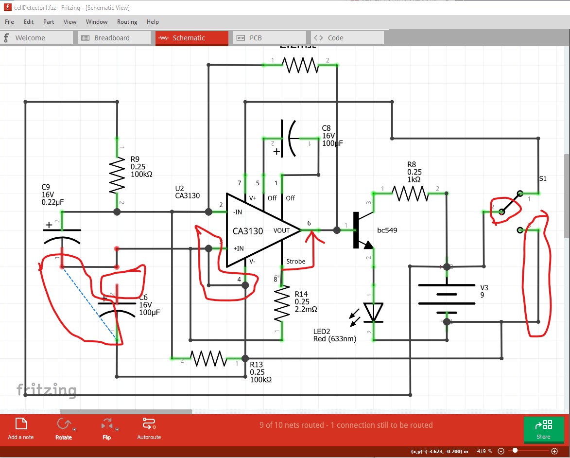
There are a number of problems here. C6 has one end not connected as does C9 (the red bar on the bottom of C9 indicates no connection, the dotted rats nest line indicates it wants a connection to V- which is incorrect.) The connection between IC pin 3 and the V- supply shouldn’t be there (that is the cause of the rats nest line from C9 to V-.) R14 should go to pin 6 on the IC not pin 8. C8 should be 47pf and a ceramic capacitor not 100UF and electrolytic and should connect from pin 1 to pin 8 not between 1 and 5. As currently connected the power switch will short the battery when turned off so delete that wire and leave pin 3 of the switch unconnected.
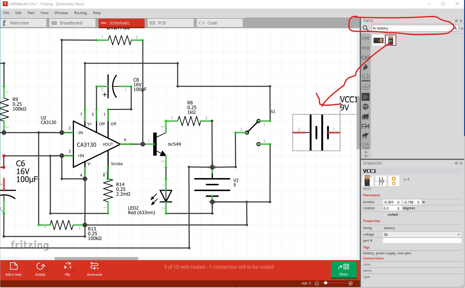
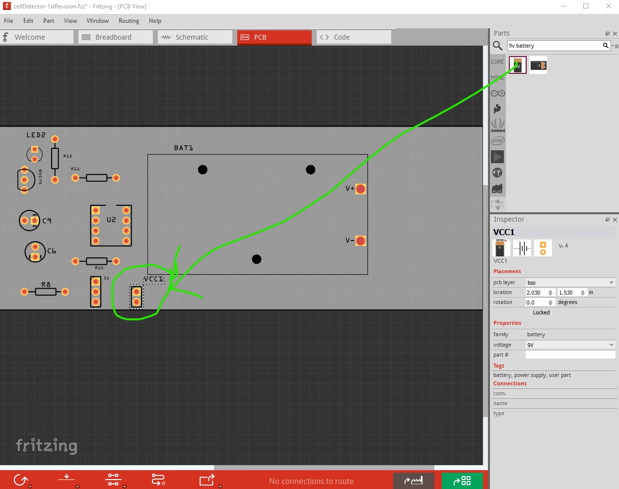
There needs to be a two pin header to attach the battery to the circuit as well, at present there is no where to connect the battery to. Easiest solution there is to replace the current schematic only battery symbol with the 9V battery in core parts which has the necessary two pin connector in pcb like this

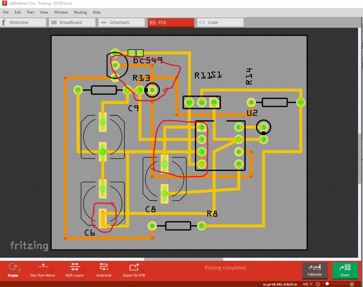
Replacing the battery in schematic will make the needed connections in pcb. In pcb, the capacitors are SMD (which are hard to hand solder) I would recommend changing to through hole, same with the LED. C6 bottom pin is unconnected (its connector is red indicating no connection.) Pins 1 to 4 of the IC are all shorted together (all of the yellow traces on the top will be copper and connect to each other.) Same with the bottom traces around the transistor, they will short as routed as there will be copper everywhere there is brown, shorting R13 at present.
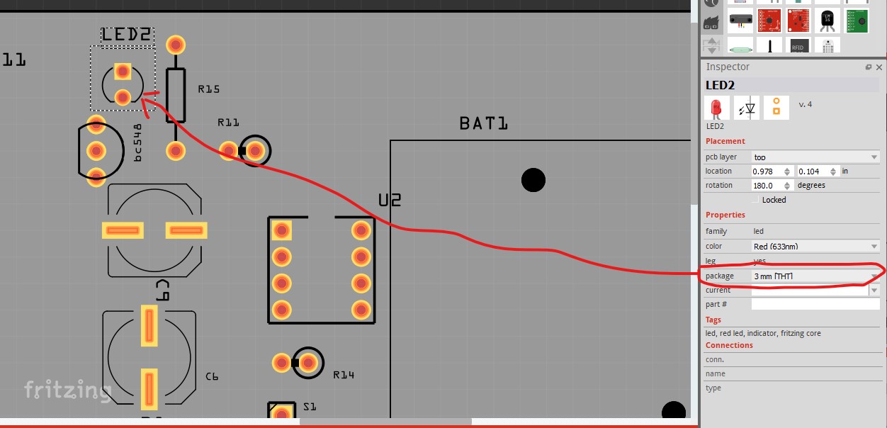
I would recommend changing the capacitors (and the LED) from SMD to through hole unless there is a reason they need to be SMD. That can be done in Inspector like this (for C6)
from

to this
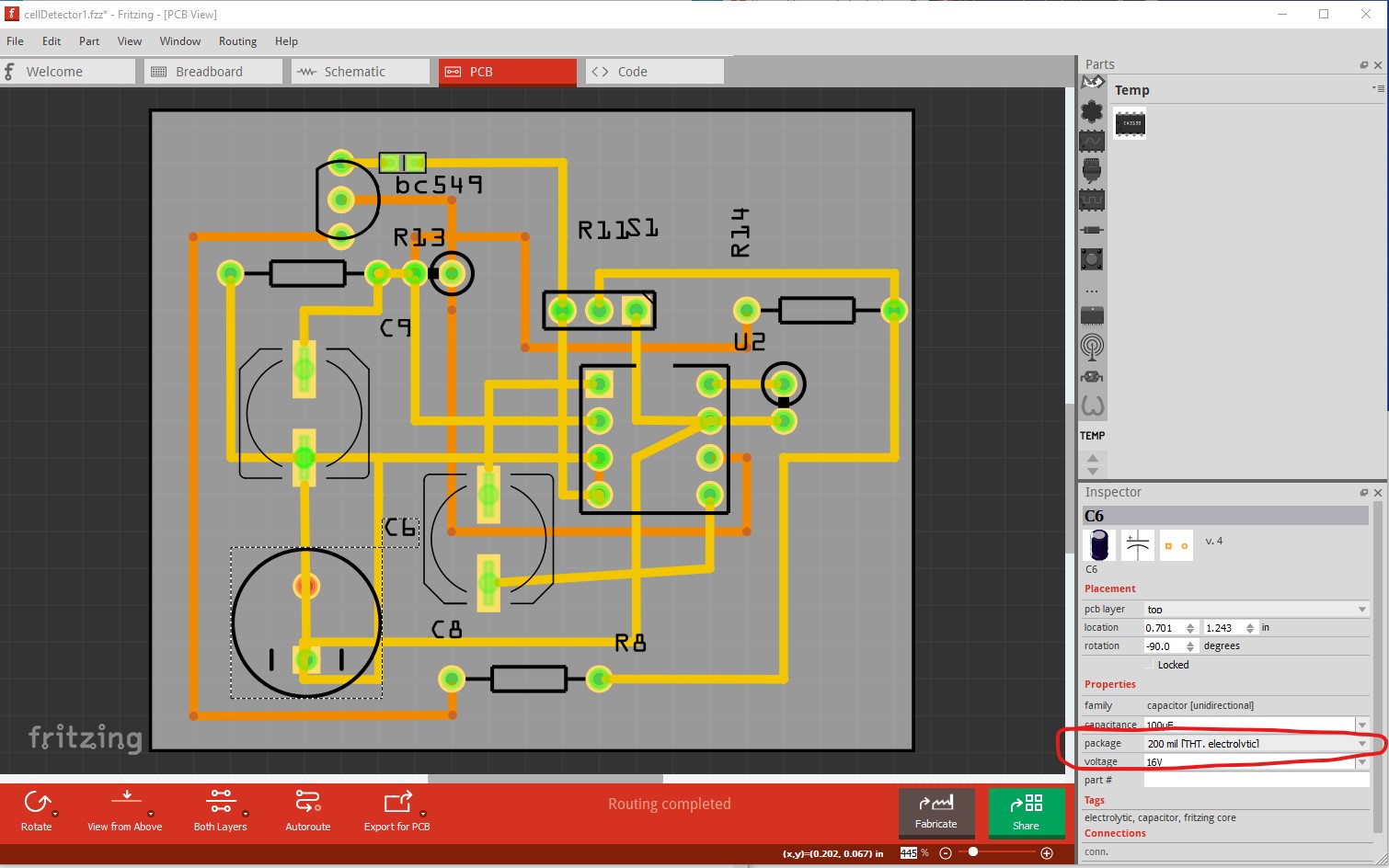
with the note that you need to check the pin spacing of the capacitor you select.Here I used 0.2in spacing but there are selections for 0.1in and 0.3in depending on the needs of the capacior you select. Soldering through hole parts is much easier than SMD. Once pcb is fixed up, run DRC in pcb view (Routing->Design Rules Check) which currently indicates your overlap problems
edit I missed at least one, R11 should connect to the V+ terminal not pin 6 of the IC, as noted R14 should be going there. I would recommend making your schematic look exactly like the one in the video although my IC part has a slightly different pin layout so you need to take care the pin numbers match the original circuit pin numbers.
Peter
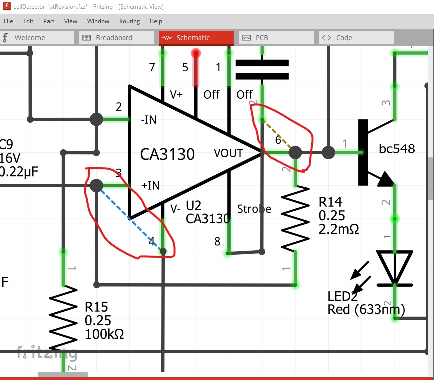
Hi, thank you Vanepp very much for responding to my requests. I have made changes to the project as you have recommended, I'm unsure of where IC pin5 connects to as it doesn't appear in the original schematic from which I initially followed ?
Schematic View Changes
- Removed connection between IC pin4(v) & pin3
- Changed c8(100uf electrolytic cap) is now c10 (ceramic - not sure how to set capacitance package to suite 47pf ?
- C10 now connects IC pin1 & pin8 not pin5
- R14 is now connected to IC pin6(vout)
- Removed Pin3 connection of switch
- Replaced voltage source for recommended 9v battery holder
- Connections c6 & c9 are now divided by IC pin3 ?
- R13 is now R15 as it lost its label somehow
PCB View Changes
- Extended board length & connected new battery holder connections
- R15 is now THT
- Deleted all wires * start fresh (I don't understand yellow and brown or rats nests)
- Fresh attempt tomorrow as it's 2am here
If you have time and wouldn't mind continuing to assist me that would be awesome I would very much appreciate you. Revised schematic project included Thank you I will attempt repairing pcb view of the project in the morning.
cellDetector-1stRevision.fzz (18.5 KB)
It is an offset adjustment pin, so leaving it unconnected is fine (in use a pot is connected between it and pin1 to adjust the op amp offset voltage which this circuit doesn’t need.)
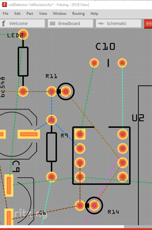
The two dotted lines in this image (blue and brown) are rats nest lines. They indicate a connection in another view (incorrect in this case) that isn’t yet routed in this view.
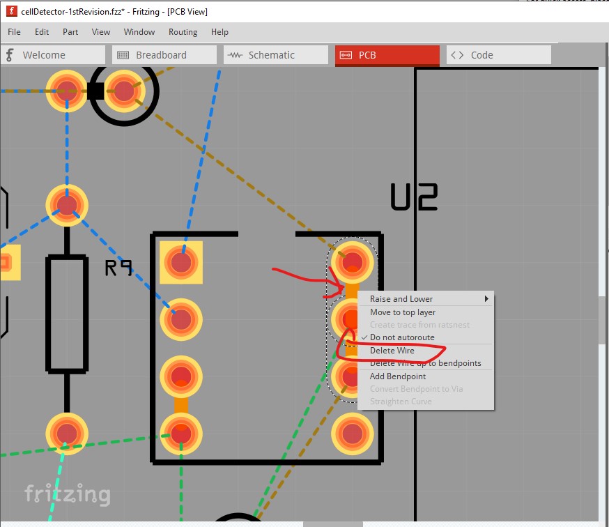
In this case these are caused by incorrect traces in pcb view (the other half of your question above):

here the two bottom layer traces are circled in red. You likely got them while moving the IC in pcb. It is very easy to move the mouse over the two pins which makes a connection between them as in this case. Right clicking on the trace and clicking delete wire deletes the wire like this which clears the problem in schematic by deleting the unwanted connection in pcb.
That in turn removes the two unwanted rats nest lines in schematic

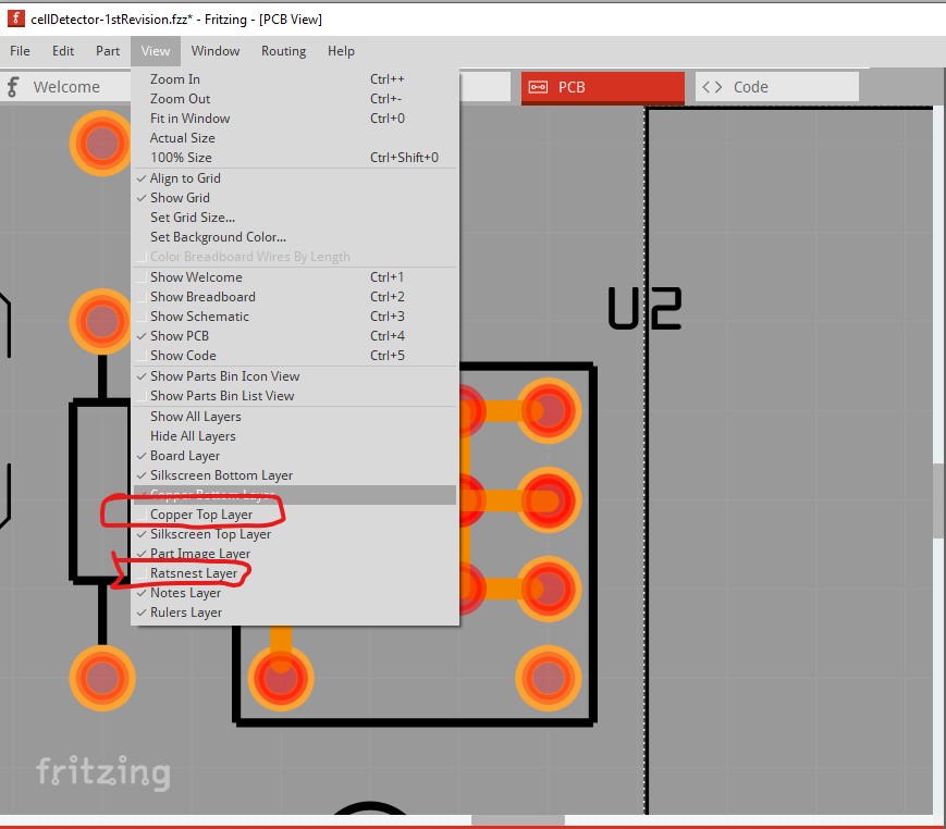
Here I have clicked on View and unselected the rats nest layer and copper top layers
to simplify the image. like this
That leaves me with the copper bottom layer (the bottom part of the two layer circuit board.) The brown lines indicate copper connections between pins. In this image I clicked and dragged the wire between the pins in the original image to make them more visible. The traces can not overlap one another (because they will short together and make unwanted connections.) The same applies to the yellow layers which show if I suppress the copper bottom layer and enable the copper top layer like this
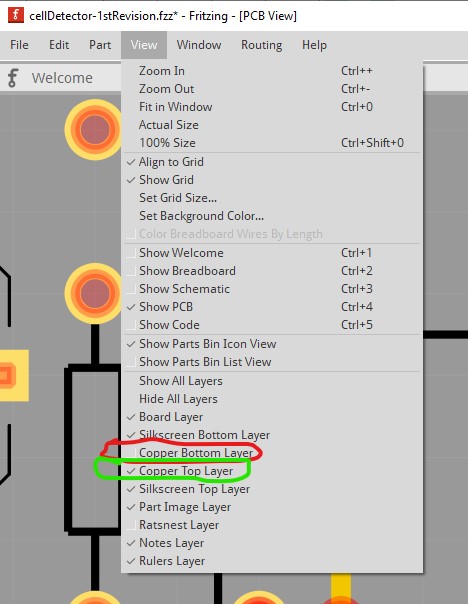
which produces this showing only the copper traces on the top of the board in yellow. Again the yellow lines here may not cross each other as they will short, but they may cross brown traces which are on the bottom of the board.
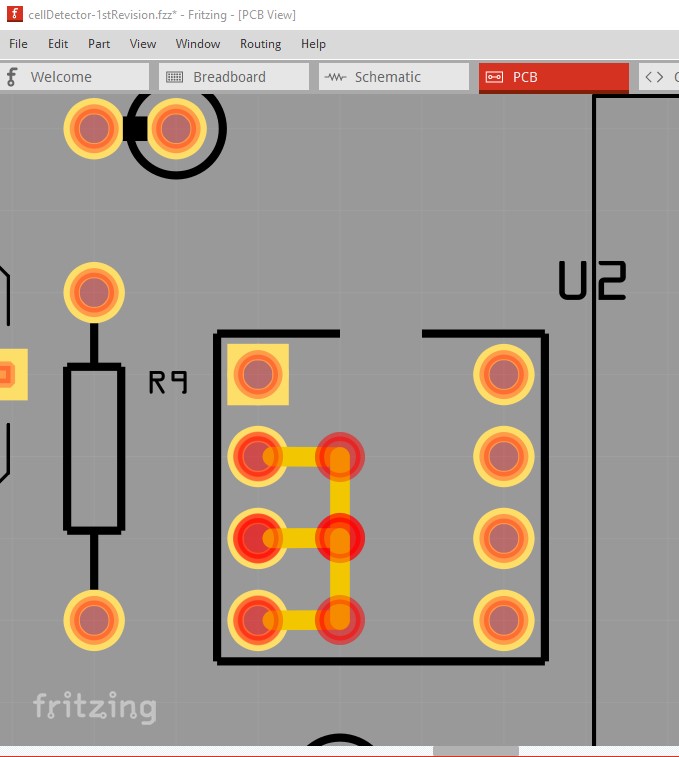
So in this image

the top 4pins are correct. pin 1 connects to pin 7 on the top layer (yellow trace) and pin 2 connects to pin 8 on the bottom layer (brown trace.) The 4 bottom pins are incorrect as all 4 pins short together because both traces are on the top layer. Now back to schematic. Here I deleted all wires (via Routing_>select all traces then hit the delete key) to leave only the components in order to suggest some changes to make schematic more readable (and more like the original schematic!)
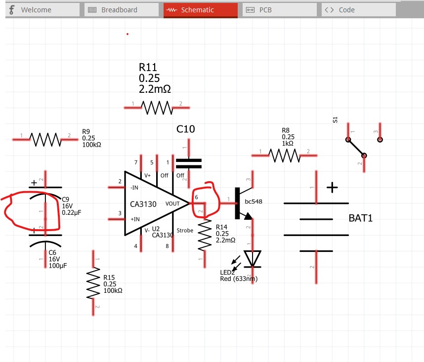
the two parts circled in red will connect like that, but I find it better to separate them and make an explicit connection between them like this.
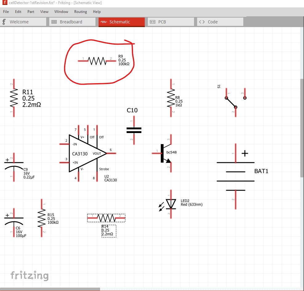
That tells me there is an extra 100k resistor (R9) that isn’t needed. Now I am going to make a couple of part changes, first I will replace C10 (which is a sparkfun part which doesn’t have a capacitance value field) with the one from core parts which does have a capacitance value field.
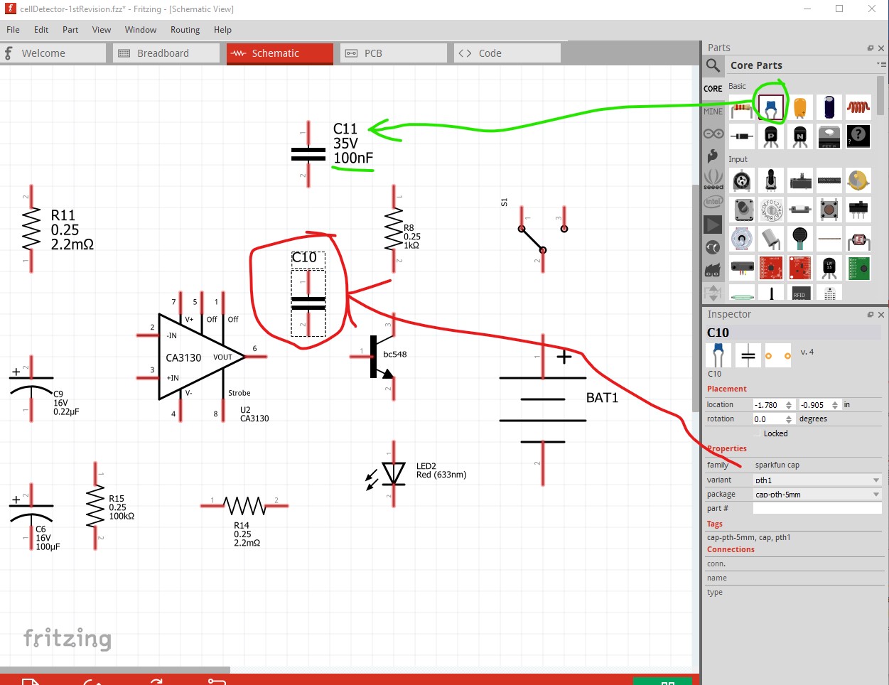
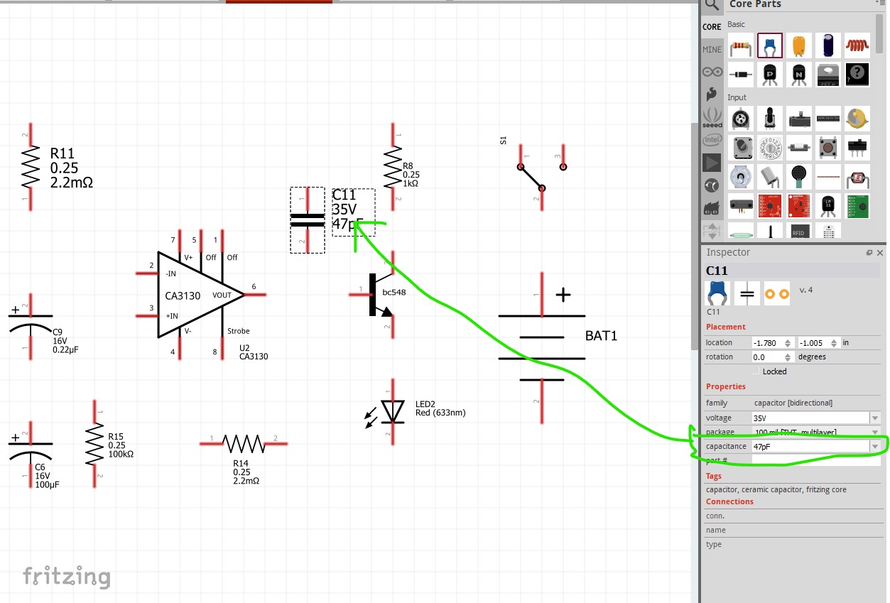
Now delete C10 and use C11 in its place, setting the capacitance value in Inspector.
Now change C9 from electrolytic to ceramic because 0.22uf is small for an electrolytic and more suitable for ceramic.
Now on to pcb to make a few changes (some of which may not be valid!)
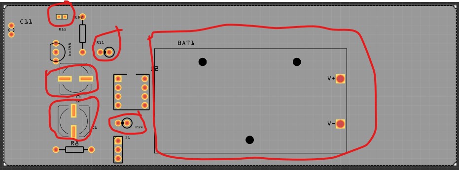
here everything circled in red I would change (the reasons are below)
The LED is currently surface mount (i.e only very small pads on the top of the board.)

I would change that to through hole as it is much easier to solder. So select LED2 and then in Inspector change its package from 603 SMD to 3mm THT which changes its pcb footprint to something easier to solder.
do the same to C6, and C9 and change R11 and R14 from 0.1in upright to standard flat on the board like R15. Which looks like this

If you intend on mounting the battery on the pcb, the current battery holder will do fine. If you want the battery to be off board (to make the pcb smaller and thus somewhat cheaper) you could change to the 9V battery in core parts which only has 2 pins on the pcb (the battery connects via wires and is fastened off board.)
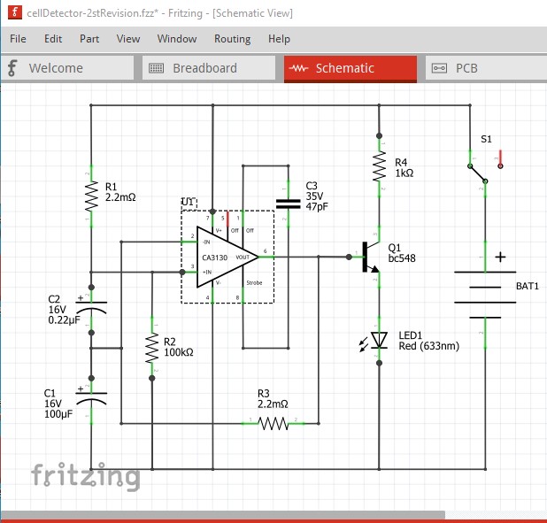
Now back to routing schematic. There I discovered a mistake in the CA3130 part which I have corrected and replaced (and will do so in the posted part in a bit!) I also see that I have pins 2 and 3 reversed from the way the original schematic specifies them so we need to make sure to connect the components to the correct pin numbers not as the originnal schematic showed. Finally with schematic finished, I renumbered the parts to be in order starting at 1 for each type of part by editing the label values. Doing all that results in this
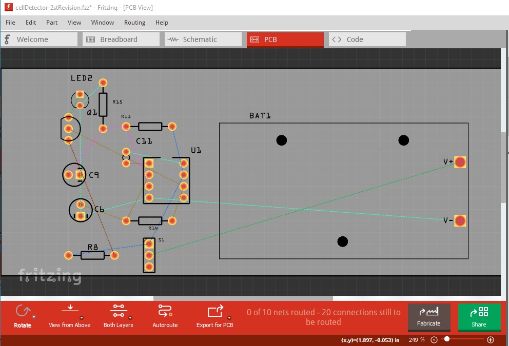
Now we switch back to pcb view and move things around to make routing the pcb as easy as possible. Initially pcb looks like this
The first change is rotate the battery 180 degrees to make the traces shorter.
Then rotate c3 90 degrees clockwise and move it to the top of the IC. Move the other parts around to make the routing as easy as possible (when you come to route it you may want to move things more if that will make the routing easier!) All these changes are in this sketch
cellDetector-2stRevision.fzz (16.5 KB)
Peter
1 Like
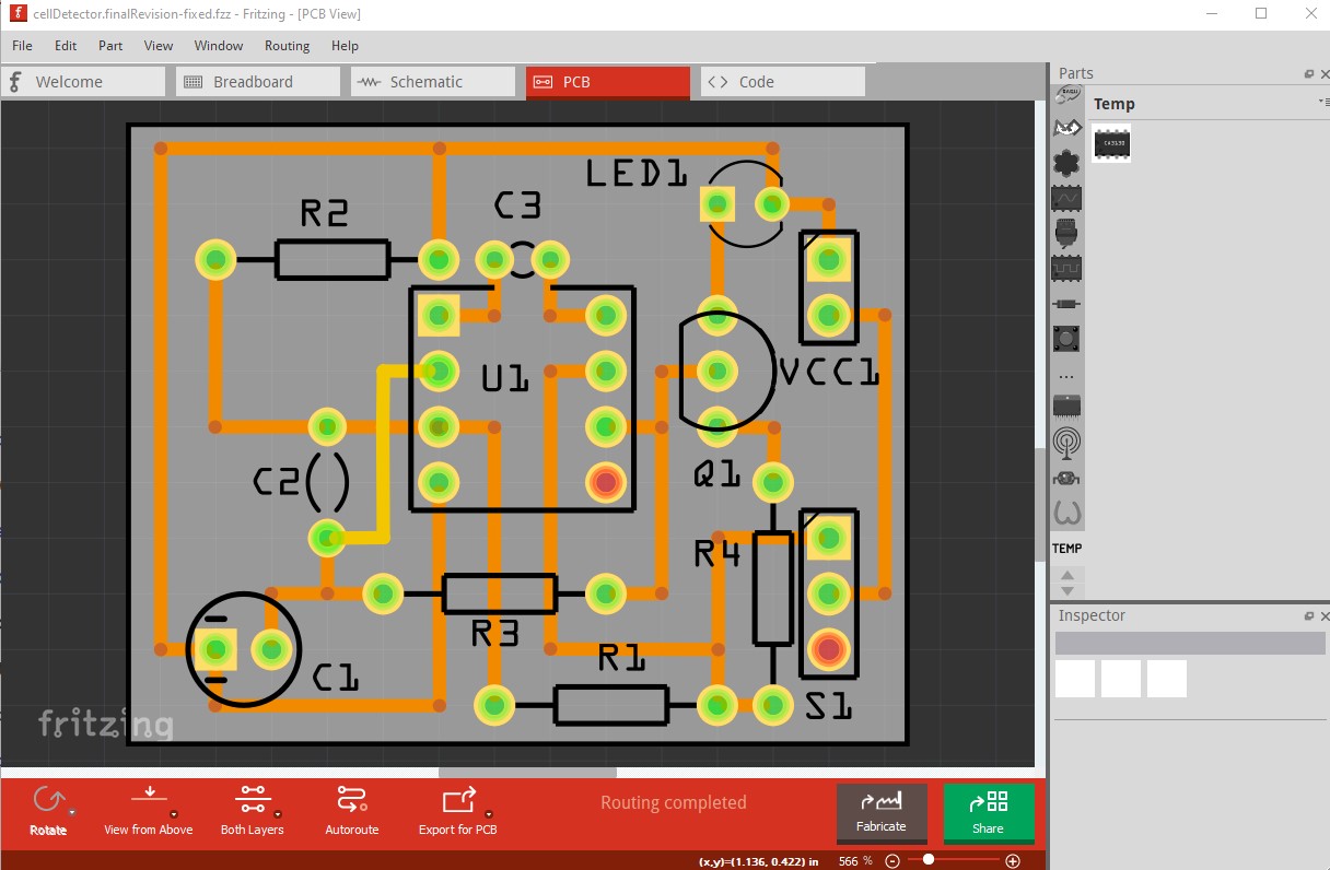
Thank you Peter for all of your assistance and detailed information, I have a better understanding of the software features and how to use fritzing :slight_smile: This is the finished project, DRC passes without error. Hopefully it functions correctly once made.
PCB
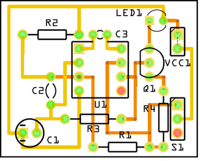
Project : cellDetector.finalRevisionfzz.fzz (28.1 KB)
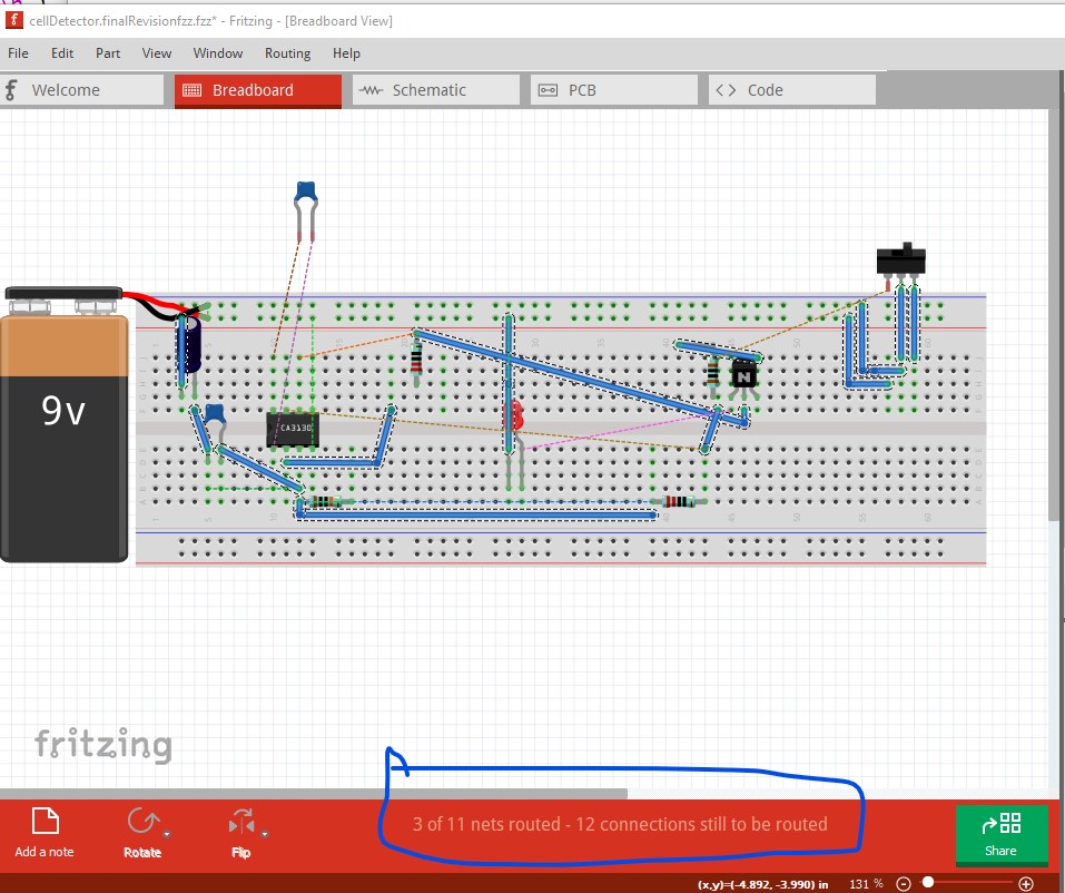
OK, still a few problems here. While DRC does indeed pass and pcb is correct, there is a short between power and ground (caused by breadboard) and indicated by no routing complete message.
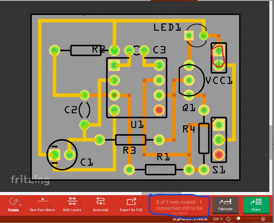
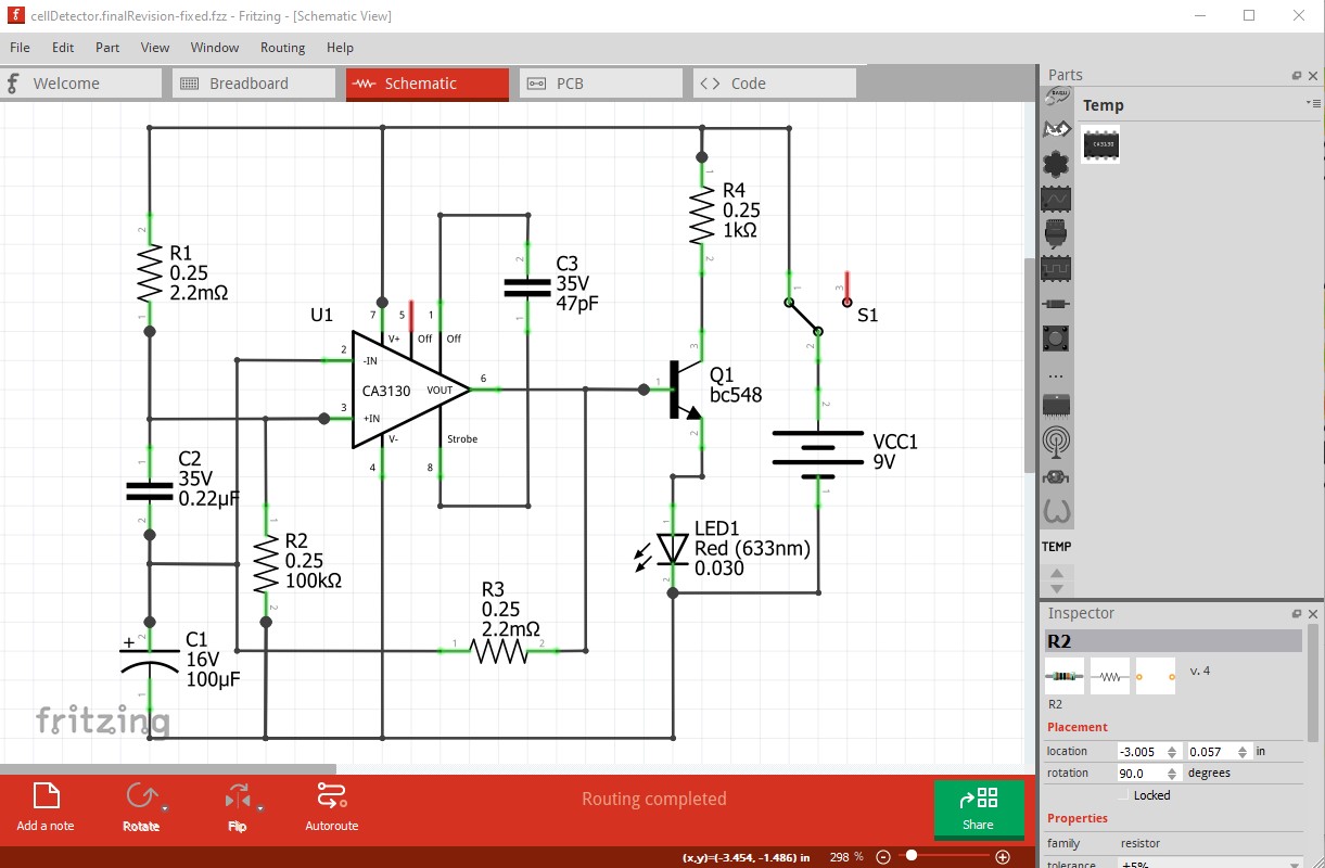
In this image (circled in blue at the bottom) we see 8 of 9 nets routed instead of routing complete. The missing net is circled in red, where there is a short across the battery. A similar thing shows up in schematic
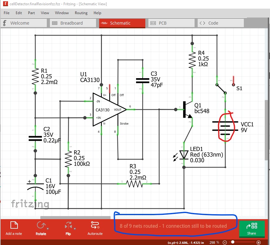
a rats nest line across the battery and no routing complete message. The problem is in breadboard
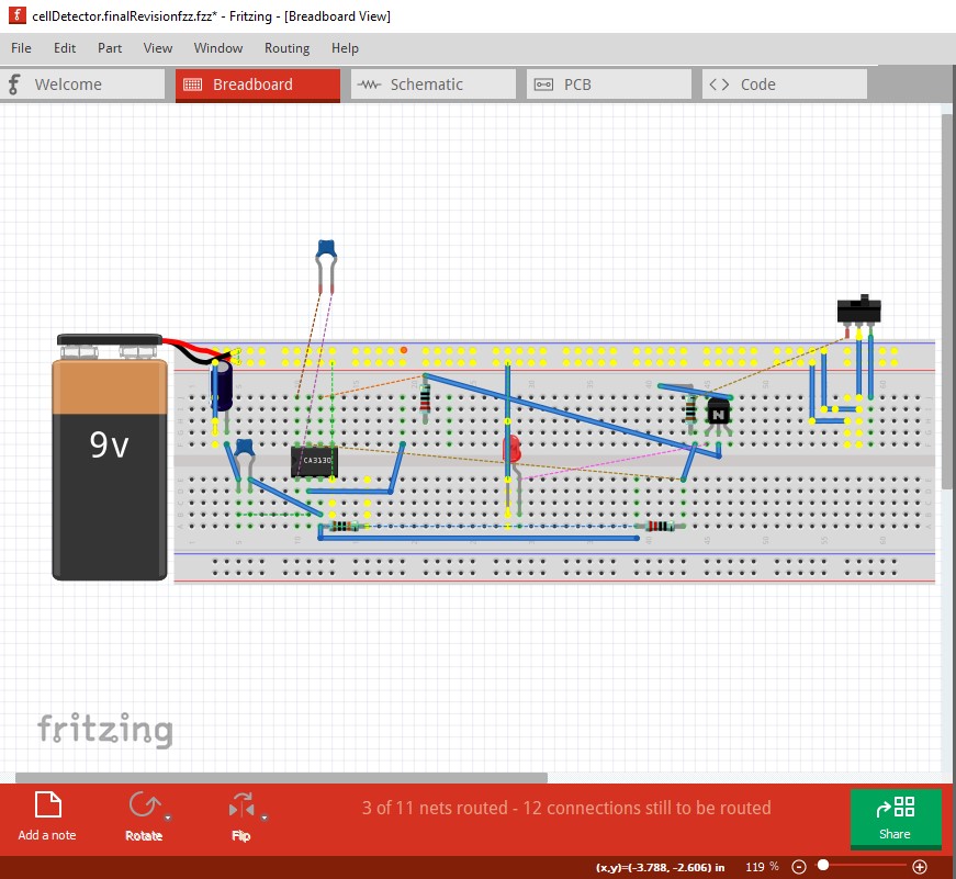
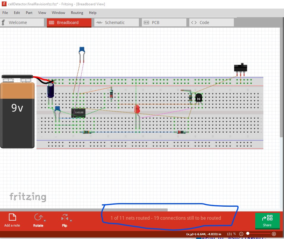
Here I clicked on a pin on the power rail, and as we see both power and ground light up indicating a short between them. To fix this in breadboard I clicked Routing->select all wires which creates this
with all the wires selected. Then I hit the delete key to delete all the wires. That produces this
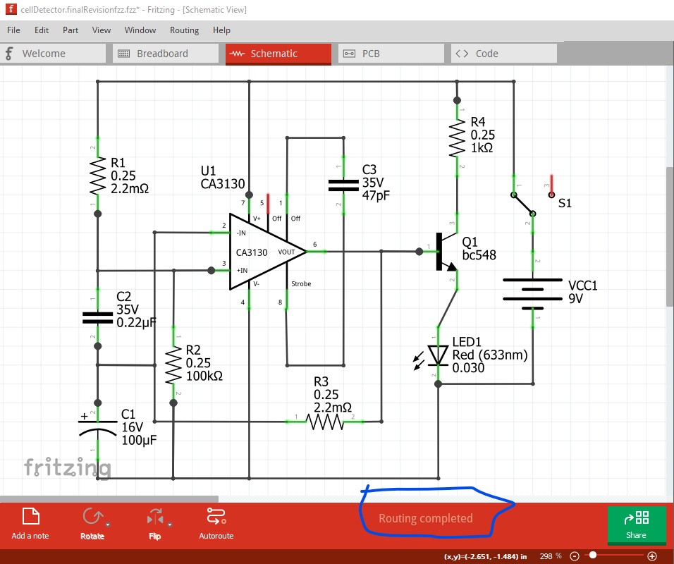
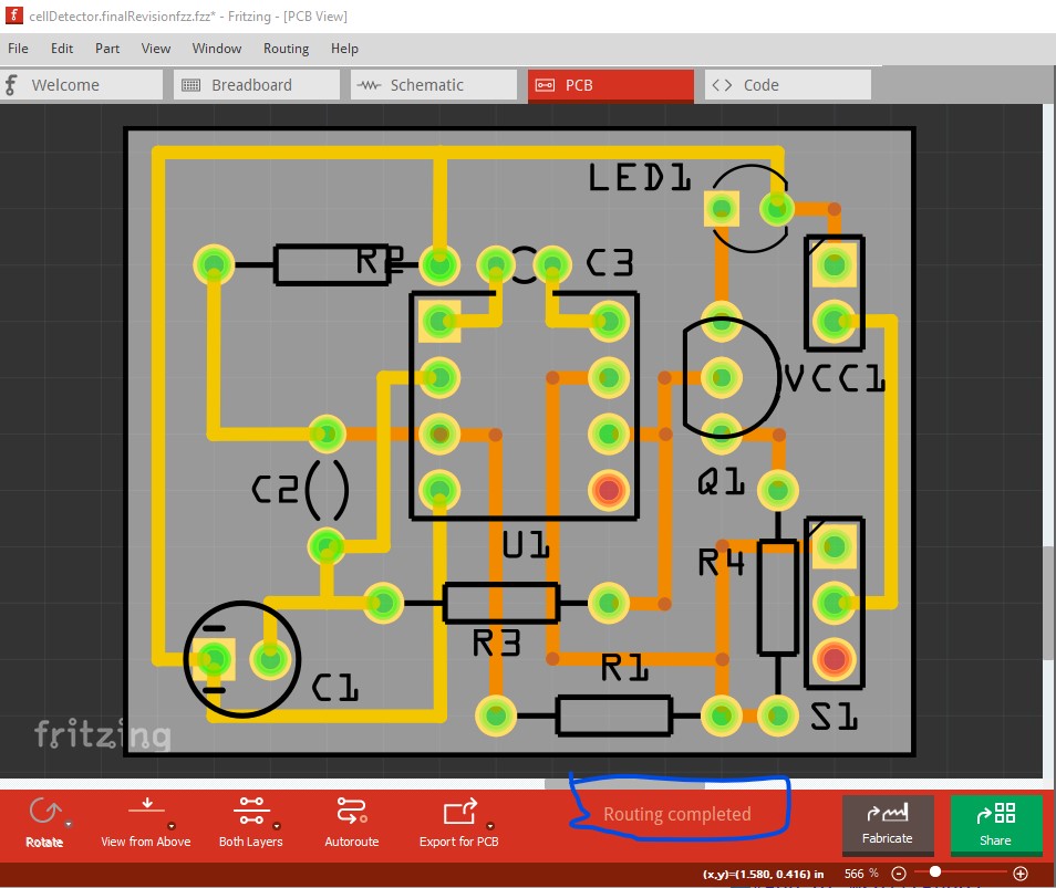
still one net routed (probably two components on the breadboard) but now schematic and pcb are correct
Then I arranged the components on breadboard and routed them according to the rats nest lines to produce this new sketch with all three views correct. You can now wire the circuit on breadboard and test it to make sure it works before ordering boards. Note I moved all traces that could be to the bottom of the board. That way they are visible even when the components are installed (although either way will work fine.)
the major change is in breadboard
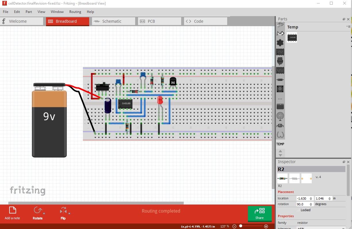
All these changes are included in this sketch
cellDetector.finalRevision-fixed.fzz (26.9 KB)
Peter
1 Like
This is really quite detailed, thanks a lot for sharing.
2 Likes