It looks like you have not positioned the hole parts correctly. They are not lining up with the marks on the pcb image, and the bottom ones are overlapping the edge. Possibly because the PCB was moved after the holes were placed. Once something is where you want it to stay, lock the part to prevent it from accidentally be moved while working on the rest. It looks like you locked the holes, but not the PCB.
Autorouting does not do DRC, so it may not leave the needed clearance. You need to adjust the trace positions after autorouting. That is normally small tweaks going around corners, and sometimes moving out a little from a row of connections. Anytime I use autorouting, I do a full cleanup of the results. To straighten unneeded zig zags, remove extra vias, adjust via positions to allow more traces to be straightened, change some obvious clumsy routes. The more you can (correctly) manually route first, the better autoroute works.
Any individual trace can have the width adjusted. You can select an autorouted trace, then change the width in inspector, or you could route specific traces manually, with the needed width, before autorouting. Any existing trace can be marked as “Do not autoroute”, (including previously autorouted traces) so autorouting will leave it alone, and work around it. May need to adjust trace positions to compensate for increased size of the specific traces. For this, I would start by using (extra) thick traces for ground across the bottom (all bottom layer), and extra thick traces for the 12V across the bottom (all top layer), mark them as do not autoroute, then run autoroute again.
You can also effectively increase the ground connection trace sizes using ground fill. After manual or automatic routing is finished.
It looks like you are using a custom image for the PCB. The image used for that will need to be modified to add the room above the header pin rows.
You probably do not need the extra space. It looks like you only need it for the one trace. That should be able to be routed differently, to not use that outer path. Probably with an extra via or 3.
You could make the breadboard view easier to follow. You did a good job of routing the wires (though parts could be simplified), but adjusting some of the wire colors could improve it. For starters, change all of the ground wires to black, and all of the power wires to red. Maybe each of the different voltages to different colors instead. That done, change some of the middle wires in the groups to different colors, to make it easier to keep track of which wire is being followed.
I would have started with the schematic view, which you have not used. Looking at the breadboard view, I am not SURE that various voltage rails are connecting where they are supposed to.
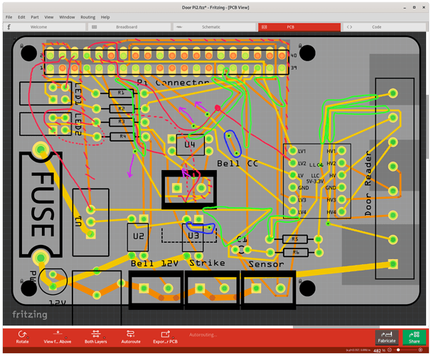
Here is a copy of the sketch with the mounting holes moved, suggested manual routing of the ground and 12v traces, and autorouting. No cleanup has been done after that. I marked up a screenshot to show some of the places that cleanup can be done.
Blue circles: change to other layer and remove vias
Red line/Red slashes: alternate route for trace
Dashed Red line: alternate alternate route
Green circles: straighten trace
Purple arrow: move via (to make more room for other traces)
More would be possible. Doing some of the alternate routing traces manually, marking them as do not autoroute, and rerunning autoroute might get some of the other things cleaned up (for free). This is an iterative process. Clean some of the more obvious pieces up, and see that it looks like.
Door Pi2.fzz (157.7 KB)
