I look for a Fritzing part of the raspberry pi compute module 4.
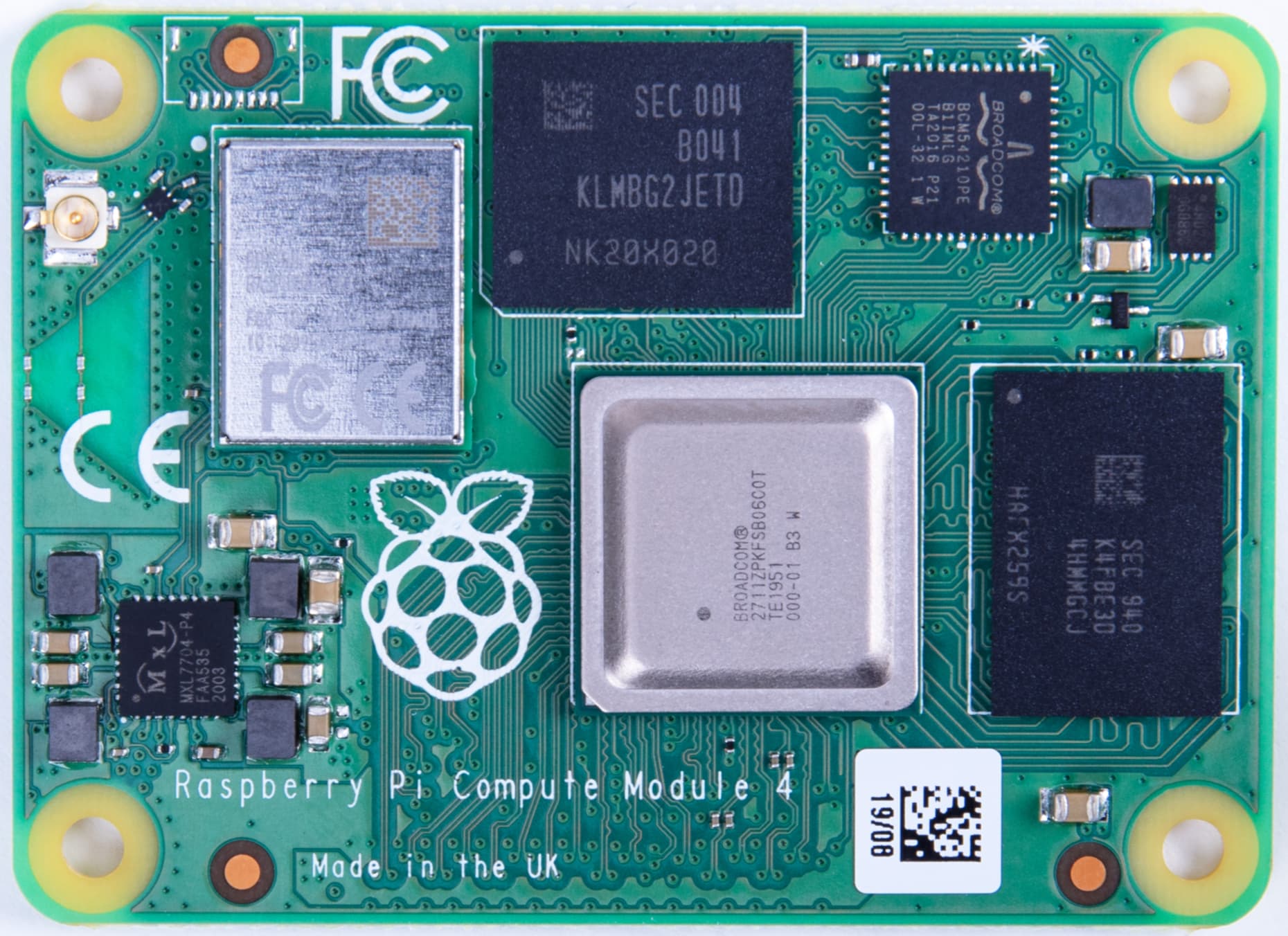
Here is a carrier board in KiCad:
top view:
Here is the datasheet:
most important is page 15 where the schematic is placed.
Thank you for your time and help!
I look for a Fritzing part of the raspberry pi compute module 4.
Here is a carrier board in KiCad:
top view:
Here is the datasheet:
most important is page 15 where the schematic is placed.
Thank you for your time and help!
Hi @Jschoerner
By the way work as started
Hi @RAPTOR7762 ,
Thank you very much!
These should be the parts you want
Raspberry Pi CM4 (0.1in).fzpz (49.8 KB)
Raspberry Pi CM4 (0.4mm).fzpz (32.7 KB)
The first part is the CM4 on a 0.1 pitch breadboard adaptor for easy wiring. The second part is just the board itself
Good work, looks great! For me the pcb view would be very important, unfortunately I can´t use your part in pcb view. Is it because of an error by my Fritzing applikation or is it not implemented?
PCB view has been suppressed in the released parts. There isn’t any documentation that I can see other than the referenced KiCad project on github and I don’t know how to get the measurements required from that to make a pcb image for Fritzing so I expect adding pcb is going to be difficult. There appears to be a snapmagic footprint available but they do not support Fritzing. A google search finds an Eagle lbr file but no .brd file (which Eagle2Fritzing requires.) If you can find an Eagle .brd file for the board I can try and see if Eagle2Fritzing will create a Fritzing footprint but I don’t see one currently.
Peter
You appear to be in luck. I was able to find the cm4 footprint in Kicad and get a png file of it which should allow me to create a pcb (which may or may not be correct enough.)
Peter
OK pcb has been added and the resulting part sent to @RAPTOR7762 to be replaced in the posted parts.With enough care it is possible to make DRC with default rules pass (although you need to set the grid size to 0.25mm, and place the 8mil traces very carefully.) PCB was created from the measurements from the Kicad part but I don’t have one of these and thus can’t check it. so you need to print the pcb footprint out at 1:1 scale (the default) and compare it to a real part. Given the 0.5mm pitch I’m not sure how successful that will be. The mounting holes are not drilled by default but are only on silkscreen. If you want mounting holes (which for safety you probably will, as without then the board will likely rip the connectors off the pcb!) you will need to drag the core parts→pcb→hole part in to your sketch, place it over the holes in silkscreen and set the size appropriately. Below is a test sketch with pcb routed and passing DRC.
routing-Sketch.fzz (156.0 KB)
Peter
OK I have edit my post and replaced the part
Great! I will update you when I have tested it.