That may be my fault. Lxml is one of the few programs that obeys the space:preserve command and leaves the blanks in the xml. It annoys me when I’m editing so I delete the space:preserve (then lxml deletes the redundant spaces). I think Illustrator wants the space:preserve to work, so probably adding it back in at the top of the svg would have saved those hours of work. Sorry about that …
So far as I know you can’t make oblong pins as a single path. You can make a circle as a path, and gerber will drill a hole. Every thing I have tried with oblong paths with holes in them doesn’t drill the holes in gerber processing. In this case there are the paths (46 of them) then 46 circles (which are the connectors) which over lay the paths. As a bonus, changing the radius of the circle will change the hole size (at least in Inkscape) easily without having to recalculate the path to change the size of the circle. As I said this is the only oblong pad that I know of that works in Fritzing (at least and drills holes in gerber output.) I’ll look over your changes now.
edit:
Lots of problems!
Breadboard:
layerId should be breadboard (not breadboardbreadboard which is specific to breadboards and may trigger unexpected code)
It is desirable that all the connectors be at the very bottom of the svg in group schematic like this
(from the original extracted from vi)
    <circle
      cx="329.37469"
      cy="171.59525"
      id="connector0pin"
      r="29"
      fill="none"
      stroke-width="10"
    />
    <circle
      cx="329.37469"
      cy="71.609756"
      id="connector1pin"
      r="29"
      fill="none"
      stroke-width="10"
    />

 ...
    <circle
      r="30"
      cy="1430.1786"
      cx="428.83005"
      id="connector45pin"
      fill="#ffffff"
      stroke="#d4aa00"
      stroke-width="10.41666985"
    />
    <circle
      id="connector46pin"
      cx="528.82977"
      cy="1430.1786"
      r="30"
      fill="#ffffff"
      stroke="#d4aa00"
      stroke-width="10.41666985"
    />
  </g>
</svg>
The reason being that I have python scripts (as yet unpublished) that will number the connectors (when it finds the first item with an id of “connector”) in sequential order which reduces the work of defining connectors or renumbering them to add connectors in the middle. I would like to see all Fritzing svgs end up this way to allow tools to easily manipulate the svgs. For the same reason, I removed all instances like this

which is a stray unused connector which will confuse the scripts. This appears to be an invisible rectangle which could be removed.
This one I will remove becasue it shouldn’t be there (don’t know where it came from, it appeared when I ungrouped the svg.)

I have renamed all the connecotrxxpin_yy to polygon-123 and moved all the connectors to the bottom, then regrouped (but left the space:preserve)
<?xml version="1.0" encoding="UTF-8" standalone="no"?>
<svg
   xmlns:dc="http://purl.org/dc/elements/1.1/"
   xmlns:cc="http://creativecommons.org/ns#"
   xmlns:rdf="http://www.w3.org/1999/02/22-rdf-syntax-ns#"
   xmlns:svg="http://www.w3.org/2000/svg"
   xmlns="http://www.w3.org/2000/svg"
   xml:space="preserve"
   enable-background="new 0 0 245.968 164.34"
   viewBox="0 0 246.0628 164.24401"
where the xml:space=“preserve” is probably what Illustrator was unhappy about being deleted in the original svg. See of Illustrator likes this svg I guess.
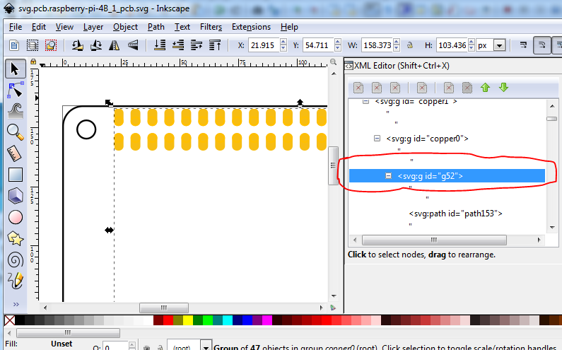
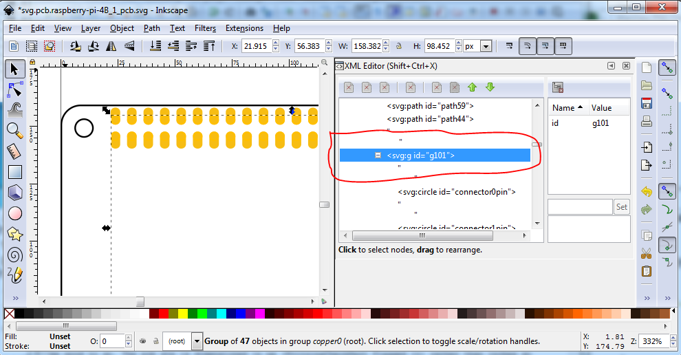
The fzp file still has the layerId as breadboard, so the breadboard svg layerId would have been wrong (FritzingCheckPart.py would have complained about it.) So see if this works in Illustrator and we should be good to go. The pcb svg is dimensioned in px (FritzingCheckPart flagged it) rather than inches so correct that. I see what you mean about no holes in pcb, something went wrong. That isn’t the pcb svg that is in the original file. It is missing all the connectors and is dimensioned in px. I’ll replace it withe the original correct pcb svg rather than try and fix it. Something (parts editor os a good candidate!) inserted some groups in to the copper0 group. This is part of the reason I don’t use parts editor it loves multilevel groups which screw things up!):
Ah! Something has replaced the fills in the connectors with fill:none again, this will likely work in gerber just fine (as it doesn’t care) but it won’t display correctly. The original svg has this
fill:#ffffff;stroke:#ffbf00;stroke-width:0.72000003
fill:none;stroke:#ffbf00;stroke-width:0.72000003
plus the scale is incorrect as well as being dimensioned in px (so perhaps this is an Illustrator issue). the original svg has an Inkscape doc properties that looks like this:
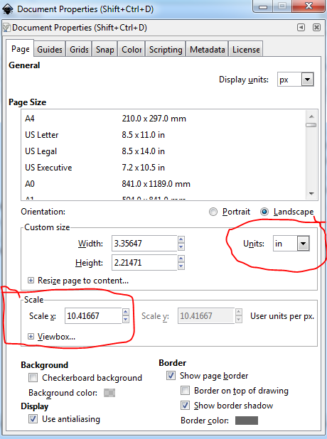
the svg in your fzpz has a document properties that looks like this (plus the extra groups and changed fill value):
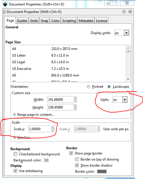
with dimensions in px (which can cause scaling problems) and the wrong scale. I’ll copy back in the original pcb svg. Just discovered the same thing happened to breadboard, it too is in px and at the wrong scale. It looks like Illustrator is changing the dimensions and scale when it edits Inkscape documents. We need to figure out how to stop it from doing that and get it to write the correct dimensions and scale because we eventually (when I finish an upgrade) want to put FritzingCheckPart.py in to the parts acceptance tool chain and it will insist on the correct scale and dimension settings. Plus I just found more problems. the scale in breadboard is indeed wrong, the pins are no longer on .1 boundaries:
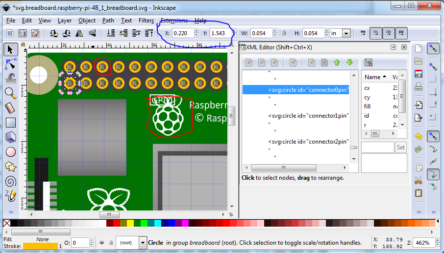
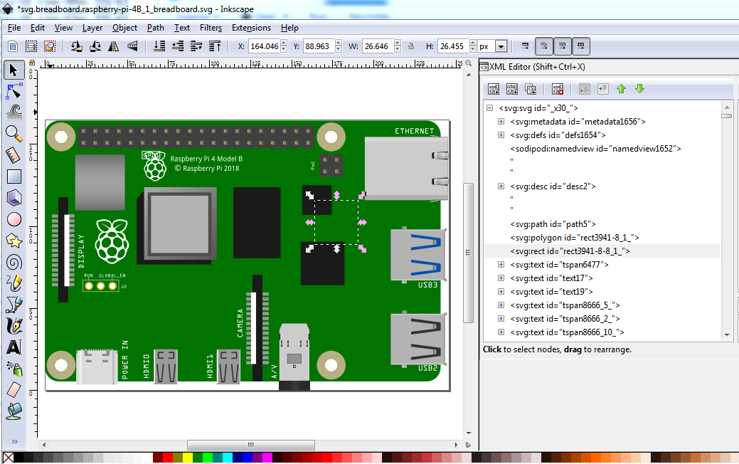
the copper circles were set invisible (fill:none and stroke:none) in the original and now have values again and the rpi logo circled in red should have been deleted. As well the xy coords of connector0 displayed here are no longer scaled on 0.1in boundaries when I display connecotor1 (presumably because of the dimension being in px with an unknown DPI setting.)
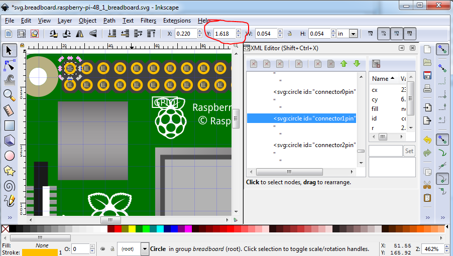
The y coords here should be 1.643in not 1.618in. It is getting late here, I’ll poke at this some more tomorrow and see what I can do. I can probably rescale this svg and remake the changes in the original in Inkscape, but I expect we need to figure out how to get Illustrator to not change the scale and set the dimensions to px to successfully interoperate with Inkscape.
Peter