Nope still appears to have both problems. Let me try and make them clearer:
This is the lack of terminalids on schematic. It manifests as the line connecting to the center of the pin definition like this in both your parts (where j1 and j2 are a 2 pin and 1 pin header connector from core parts):
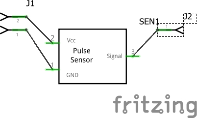
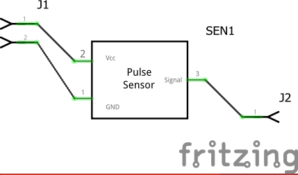
what you want is this (from my new version):
which is produced by changing this in the schematic svg:
   <path
      gorn="0.3.0.0.5"
      d="M 7.0965554,332.20642 0,332.20642"
      stroke="#696969"
      stroke-opacity="1"
      stroke-width="0.64"
      id="connector1pin"
      fill="#696969"
      fill-rule="evenodd"
      stroke-linecap="butt"
      stroke-linejoin="miter"
    />
    <path
      gorn="0.3.0.0.6"
      d="M 7.0965554,346.63323 0,346.63323"
      stroke="#696969"
      stroke-opacity="1"
      stroke-width="0.64"
      id="connector0pin"
      fill="#696969"
      fill-rule="evenodd"
      stroke-linecap="butt"
      stroke-linejoin="miter"
    />
to this:
   <path
      stroke-opacity="1"
      stroke-linejoin="miter"
      stroke-linecap="butt"
      stroke-width="0.63999999"
      stroke="#696969"
      fill-rule="evenodd"
      fill="#696969"
      gorn="0.3.0.0.5"
      d="M 7.0965554,332.20642 H 0"
      id="connector1pin"
    />
    <rect
      stroke-width="0"
      fill="none"
      height="0.69999856"
      x="3.5527137e-015"
      gorn="0.1.29"
      width="0.72000015"
      y="331.8197"
      id="connector1terminal"
    />
    <path
      stroke-opacity="1"
      stroke-linejoin="miter"
      stroke-linecap="butt"
      stroke-width="0.63999999"
      stroke="#696969"
      fill-rule="evenodd"
      fill="#696969"
      gorn="0.3.0.0.6"
      d="M 7.0965554,346.63323 H 0"
      id="connector0pin"
    />
    <rect
      stroke-width="0"
      fill="none"
      id="connector0terminal"
      y="346.2197"
      width="0.72000015"
      gorn="0.1.29"
      x="3.5527137e-015"
      height="0.69999856"
    />
which adds a .01 inch rectangle as the terminalid which is centered on the end of the pin where the line connects (as noted without it, the connection defaults to the center of the pin so .05 in from where it should be). Then you need to set the layer id to schematic by making a group of the entire image and naming the resulting group schematic. As noted all lacking this breaks is exporting the sketch as an svg (the part will be missing).
  <desc
       id="desc3">
       <referenceFile>Pulse_Sensor_c124af3144d0973be29c3879c68bd19a_2_schematic.svg</referenceFile>
  <g
    transform="translate(0,-324.1879)">
    <g>
      <g
        gorn="0.3.0.0"
to:
  <desc
    id="desc3">
    <referenceFile>svg.schematic.Pulse_Sensor_c124af3144d0973be29c3879c68bd19a_2_schematic.svg</referenceFile>
  </desc>
  <g
    transform="translate(0,-324.26784)"
    id="schematic">
    <g
so the top group has the id schematic as the layerid. The same needs to happen in breadboard (I did a select all and then created a new group because there wasn’t an enclosing group) with the layerid breadboard.
Peter