I am in need of a Prototype Shield V3.0 For Arduino Mega with Mini Breadboard fritzing part for a science project, for which I have searched the internet for too long, but I couldn’t find it. If you happen to have it and can share it, I would be very grateful. Thank you very much!
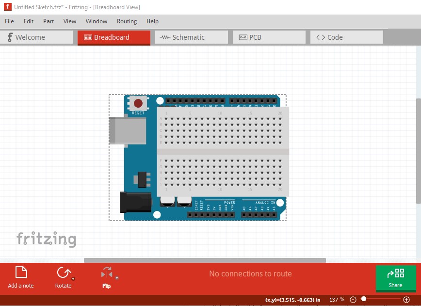
They are a lot of work to add and their position isn’t clear. Next issue is that the part will look like the image (i.e. no breadboard) as breadboards aren’t compatible within parts (the internals are different). The same effect can be had (with some inconvenience) by dragging a suitable breadboard over the part like this using a Uno as an example:
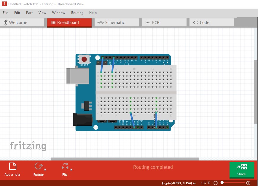
The downside is that unless you select both with a select rectangle they won’t move together. Staring from here (with some wires attached to the breadboard)
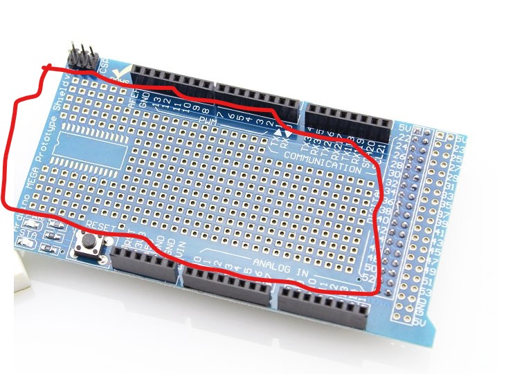
The angle is not the best, but it looks like the prototype pads at the right end are aligned with the final pin in the (top) side row of header pins. Then, the top most (short) row of pads appears to have a 0.1 inch offset from that side header row. Assuming the rest is a standard Arduino Mega shield footprint makes it possible. The surface mount pad position should not be critical, since there does not seem to be any mechanical interaction with the rest of the spacing. The hardest part there, is to get the bus right for the smd pad to prototype pad/hole. It would ‘nice’, if could drop a bare chip on that and get the connections.
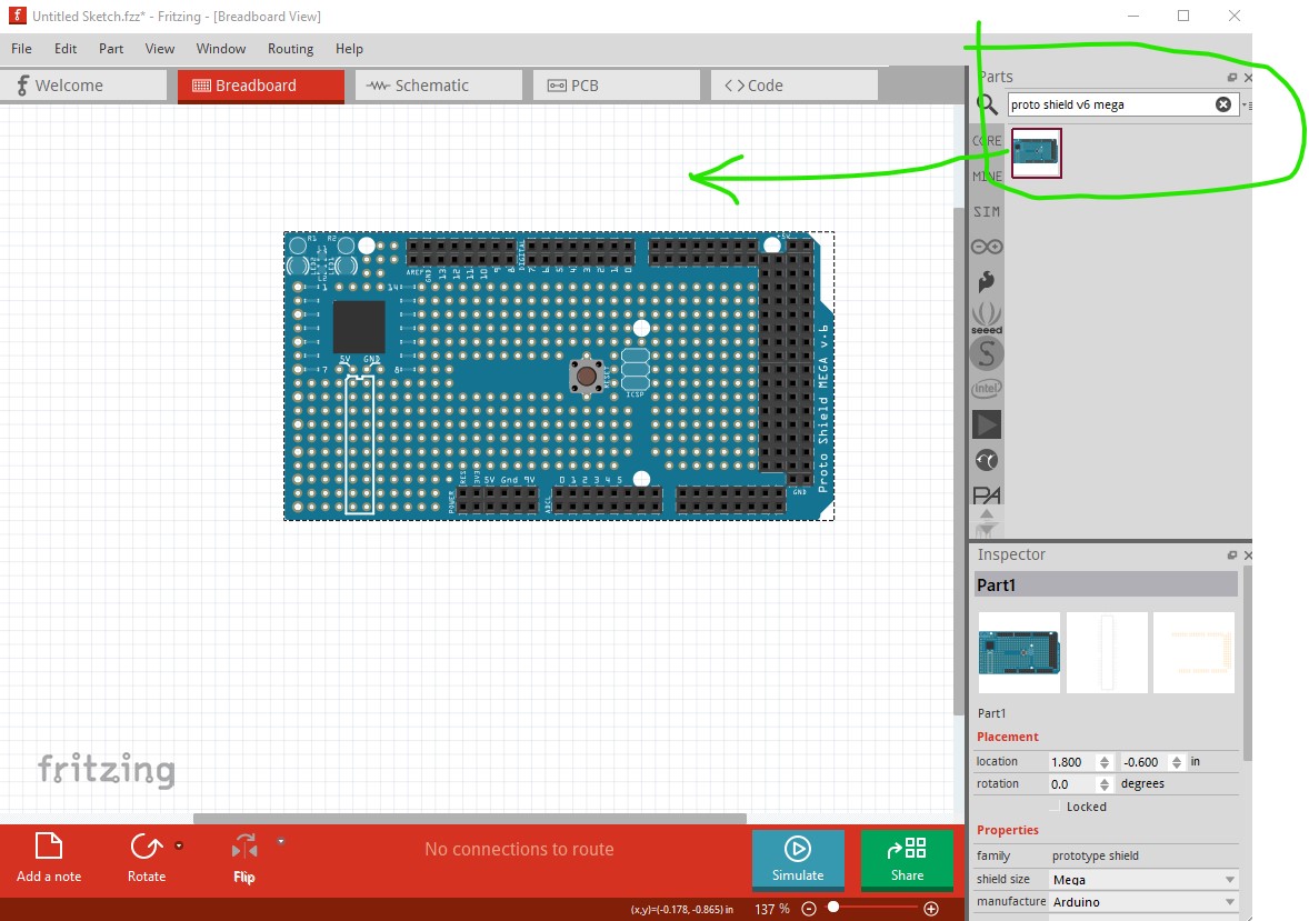
Does not help with the ‘work’ part, but should be enough for the positioning.
I agree it is likely possible (if a lot of work) to do something about the prototype area. The best outcome will be if he or she doesn’t need the prototyping area just the Mega pins and the breadboard and doesn’t mind the issue with the breadboard being separate. That is a lot less work. Just modify a copy of the mega to add the extra back connectors (if needed) or better yet use the existing mega connector for them, rather than add several hundred new connectors. Come to think of it, the proto connections are going to need to be in a breadboard part, as a custom breadboard just for this shield, as the proto area is a form of breadboard and thus needs to be in a breadboard part (I think!) to not reflect in to schematic and pcb! As far as I can see the ICSP connector is floating, it doesn’t seem to have any way of connecting to the Mega’s ICSP connector that I can see (there are more pictures in the datasheet, unfortunately none clearer though!) although I may well be missing something. I guess I’ll wait and see what the OP wants to do and/or what they need it to do and see if I am willing to try it.
Then you need to provide the pointer to a mechanical drawing for the board you want (with the warning it is a lot of work for not much gain as noted above!) As there appear to be several versions.