Program DO-201 Is it on the?

It is going to take a while to fix this up I think! The first thing I did was run DRC (Routing->Design Rules Check) which complains about many overlaps. Looking at them shows that there are two extra (and unneeded!) headers under the micro, so I need to remove those and move the pads to the correct pins on the micro itself. While at the board level this would work, it will screw up the routing database and not be correct in schematic.

Here the extra headers are outlined in red and the corresponding micro connectors in green (which are also moved 0.1in to the right to uncover the headers!)

Peter

1 Like

Yes I put “header” pins because I don’t like soldering an Arduino board. I must be able to get it back or change it. But the routing is good, on my prototype everything works. The problem is really the part that goes through the relay (diode and capacitors) And I know it’s not perfect but first of all I wanted a circuit that actually works completely ^^. The jumps and don’t bother me other than that: D. Being a beginner I did almost everything on my own “almost ahah” and I’m pretty content with the path it took. :slight_smile:

You don’t need the headers to do what you want. By default the pins for the micro are sized so they will accept a .1in header connector, so using the micro by itself works. On the actual board you can solder in a .1in header connector and plug the micro in to that. The relay looks to be a problem though. The relay draws too much current to be driven from a micro pin directly and it needs a snubber diode to suppress the back emf. The srd-05vdc-sl-c takes 71ma of current to operate, the micro pins can source or sink a maximum of 40ma, so you will need a relay driver circuit to drive the relay (a transistor and a diode is probably the simplest solution.) I’ll continue poking at it and see if I see anything further.

Peter

1 Like

For the relay I do not understand because I can make it work with my card without a problem :thinking:

I had fun redoing the routing to limit the jumpers as you advised me.

Nouveau routage.fzz (50.9 KB)

In the green square, I have reserved the place for the shottky diode.

Sorry for the late reply (I got busy yesterday!) The relay will very likely work as is, the problem is that it is straining the micro output port by drawing more current than it is rated to provide (around 70ma when the spec is 40ma max per pin and something like 200ma for all pins.) This will likely eventually damage the micro. The relay coil is an inductor, and when it shuts off it will raise the voltage (converting magnetic energy in to electrical) again potentially damaging the mirco I/O pin. A diode connected across the coil serves to short circuit that voltage spike through the diode protecting the IO pin. While I haven’t finished poking at your Nouveau routage.fzz sketch, I did notice that ground isn’t complete. The ground pin on the micro doesn’t connect to the ground on the power source. Now some questions: are the traces set to 32mil because you are home etching the pcbs and thus need wide traces? If you are having a pcb board house make the boards the traces can be much smaller and thus eliminate all the jumpers. Nice job on getting rid of most of them though! What does the photo cell do? It appears to connect in to the capacitors which doesn’t make any sense to me. Is it a switch type device that closes contacts when light falls on it and is intended to switch some of the LEDs on? The 2 red wires connected to the first capacitor board appear to be (from the picture anyway) connected to each other. What is the second red wire intended to do? It currently appears to connect to the photocell through a resistor with no connection to the micro to sense light, so I’m not sure what it is supposed to do.

Peter

But don’t apologize you haven’t done anything wrong.

I understand the value of putting a diode in this case. Thank you for your explanation.

After that I do not see how to do otherwise than by connecting the relay to the Arduino.

It is a will not to connect the GND of the card to that of the power supply. Not sure if this was a good idea, I simply avoided doing it.

I have the PCBs manufactured in a company, they are 32 simply by choice and not not by convenience.

Then I use the program’s “grid” grid for the track line-up.

If there are a few riders left, it doesn’t bother me personally. But it’s true that there were a lot of them that were easily removable so I found it interesting to redo my circuit as you had recommended.

Thanks for the compliment.

The photoresistor is output from the capacitors so that the LEDs shine less brightly if it is dark and stronger if it is daylight. The LEDs will be those of the control panel switches for space flight simulation, so very close to my face.

The first red wire is the input of the power supply, that’s why I wanted to put a diode upstream as well as to protect the power supply.
The second red wire that goes through the resistor and the photoresistor is the output that will be sent to other boards with the outputs of the GPIOs of the Arduino board for powering the LEDs of the matrix switches on several different panels. That’s why the current comes out in three places. The left and right exits will go through avionics outlets at other panels.

For this case, a simple fix is to “parallel” a couple of the microcontroller pins. Assuming you have an extra one available. It won’t be exact, but driving the relay from 2 pins would split the load, and should reduce the overall strain on the chip. Just make sure to turn both on, and both off, at the same time. Adding diodes to both pins can add safety limiting there as well.

From the previous post though, there REALLY should be a snubber diode across the relay coil. Without that, ‘spikes’ of voltage can feed back into the controller (each time the relay turns off), which is another way to cause damage there, and reduce life expectancy.

OK here are my modifications to your Nouveau routage.fzz sketch, first to clean up the sketch a bit and populate schematic. Because I am going to replace the to headers with the Arduino Micro part (which has no connectors on the NC pins) the first thing I did was place a via in the path that crosses the NC pin (circled in red here)

replace with a via as the NC connection on the micro isn’t a connection and won’t show up in schematic (a Fritzing oddity)

To make routing easier I selected View->Copper Top Layer and clicked it to suppress the top layer making routing on the bottom easier. Then I clicked on the wire and clicked delete wire to bendpoints to get it to look like this.

Then I dragged the wire to the just added via (not the connector!)

then dragged the wire so it crosses over but isn’t connected to the pad like this.

Now right click on one of the header pins that I want to replace and click Delete Minus. That deletes the selected part but leaves the traces that connect to the part (delete will delete both part and associated traces!)

Now select the end of each wire and move it away from the pin a bit like this. Sometimes when selecting and moving is difficult it is easier to delete the wire and just re route it.

Now drag a Ardunino Micro part in to the sketch and place it where the connectors were

Now click on the end of each disconnected wire and drag it back to the pin (circled in red in this image) until the connector goes from red (disconnected) to green (connected)

to end up with this. Note that the NC connection (circled in red here) has no green center as it is not a connector in Fritzing.

Now run DRC (Routing->Design Rules Check) It has a few complaints (not all of which we can fix.) If you highlight a line in the DRC report, it selects the area where the problem is and the overlap area is highlighted in red. In this case there is a pad under the jumpers when there should not be. So we need to fix that.

As well it is complaining that we have run a trace over the top of the pad (which isn’t a connector) on the NC pin on the micro. We can’t fix this so, we will ignore it (it won’t affect the final pcb)

To fix the jumper problems, move the jumper aside like this

then delete minus the vias under the jumper

and re connect the wire as we did on the Micro.

repeat for the other jumpers and rerun DRC and now it only complains about the two NC pins so all is well. Now switch to schematic and route that.

Initially schematic is a mess, so first drag and rotate the various parts to something workable.

This looks like a reasonable starting point.

As you will see I had to move things later to make room. So now start connecting and routing wires. I added the diode part which finishes the circuit and indicates the pcb routing is correct because everything in schematic appears to connect correctly. What is powering the micro remains, I had assumed it was being powered from the 12V supply, but with the grounds isolated it can’t be. Perhaps powered by a USB connection? In any case this sketch is the current board with schematic added and the changes above made. Schematic now looks like this

which came from this sketch

Nouveau routage-cur.fzz (72.0 KB)

Now for the suggested changes. First add a transistor driver and snubber diode for the relay. Then the inrush current change that Phil suggested. Here I disconnected the affected wires in pcb view and added the circuitry in schematic view. Fritzing doesn’t react well to making changes in one view (schematic here) when there are connections in another view (pcb) so it is safest to first remove any connection you are changing in pcb view. The new components are grouped below the board in pcb view because I don’t know what the space constraints are for placing them. You need to find a way to add them to the board (possibly by moving things around) then wire them up according to the rats nest lines which are reflecting their connections from schematic. In addition to that it is very desirable to have the wires from the power connectors to the relay and the capacitors, short and as wide as possible (to reduce the voltage drop in the traces.) The capacitor surge circuit is described in Phil’s earlier post. The relay driver adds a 2n2222 transistor with a 4k7 base resistor which will provide about 10ma of base current. The gain is about 100, so that will provide about 100ma of current in the collector to drive the relay. Another sr506 diode is connected across the relay coil to provide a path for the back emf when the transistor shuts off. A 1n4001 or the like would work here as well. If the transistor is too much of a problem to add, as Phil suggested you could use one of the free I/O pins to double up the drive and eliminate the transistor and its base resistor, leaving the diode across the relay coil to absorb the back EMF. I prefer the transistor method but either should work. Here is the new schematic with the changes circled in red

and the sketch with the changes in it (but pcb not routed!)

Nouveau routage-fixes.fzz (78.3 KB)

Peter

1 Like

Wow that’s a lot of a sudden, this might take me two or three days. I won’t be bored: D

I would just like to know why we can ignore some error reports and not ignore the one that goes through the NC pins?

I didn’t understand the translation for the jumper “In this case there is a pad under the jumpers when there should not be” I did them all the same on my old models and everything came out fine. (I’m not doubting you, I’m just trying not to be ignorant and understand. ^^)

I also see that you have enlarged the holes for the SR506 thank you. However, they are too close to each other. Could it be possible to remedy this defect please?

I had absolutely not thought of a transistor, simple but elegant / like. In addition to that if it is the 2n2222 I already have it in stock: DSR506

We agree that diode D2 there is no need to put an SR506? Would a low voltage diode at 1 ampere suffice?

Why is one side of diode D2 connected to GND?

I don’t understand why 5v and pin 06 are in direct contact.

And I also do not understand the diode D3 which prevents the LEDs from sending current to the power supply?
I am currently re-routing to make room for these new components.

Will the transistor work like this?

The SR506 would be at the bottom left where there are the two holes.

Nouveau routage 3.fzz (54.0 KB)

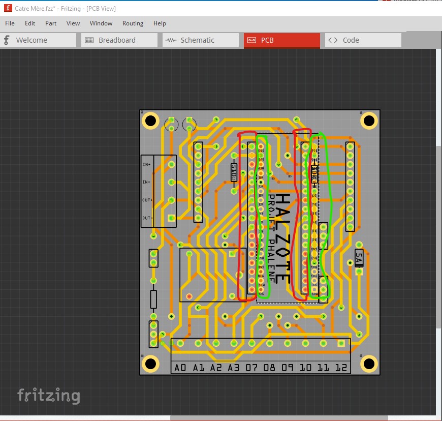
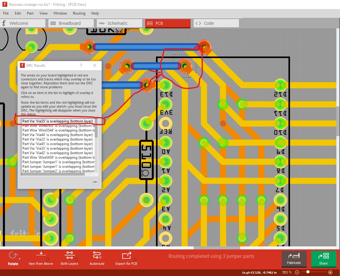
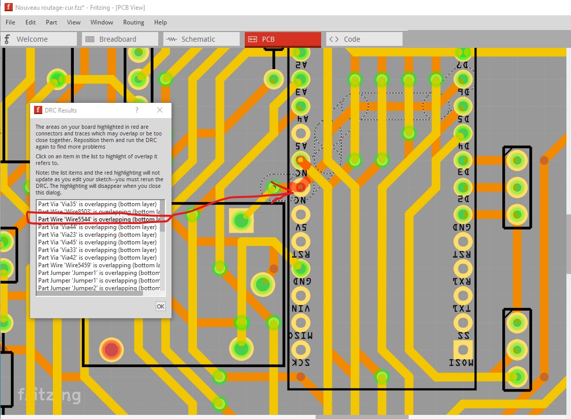
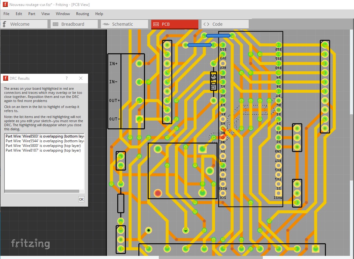
My preferred method is to eliminate all DRC errors. In this case that would mean routing the traces that cross the NC connections in the Micro so they don’t cross the NC pad. That is a lot of work for not much gain, so I elected to ignore the DRC error. It is safe to ignore it because there is no connection on the NC pad in the micro, so the trace crossing it won’t cause a problem (even though DRC thinks we shouldn’t do that.)

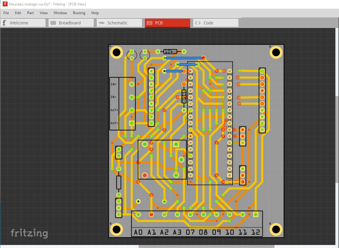
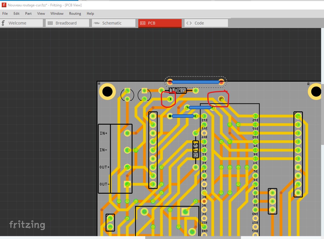
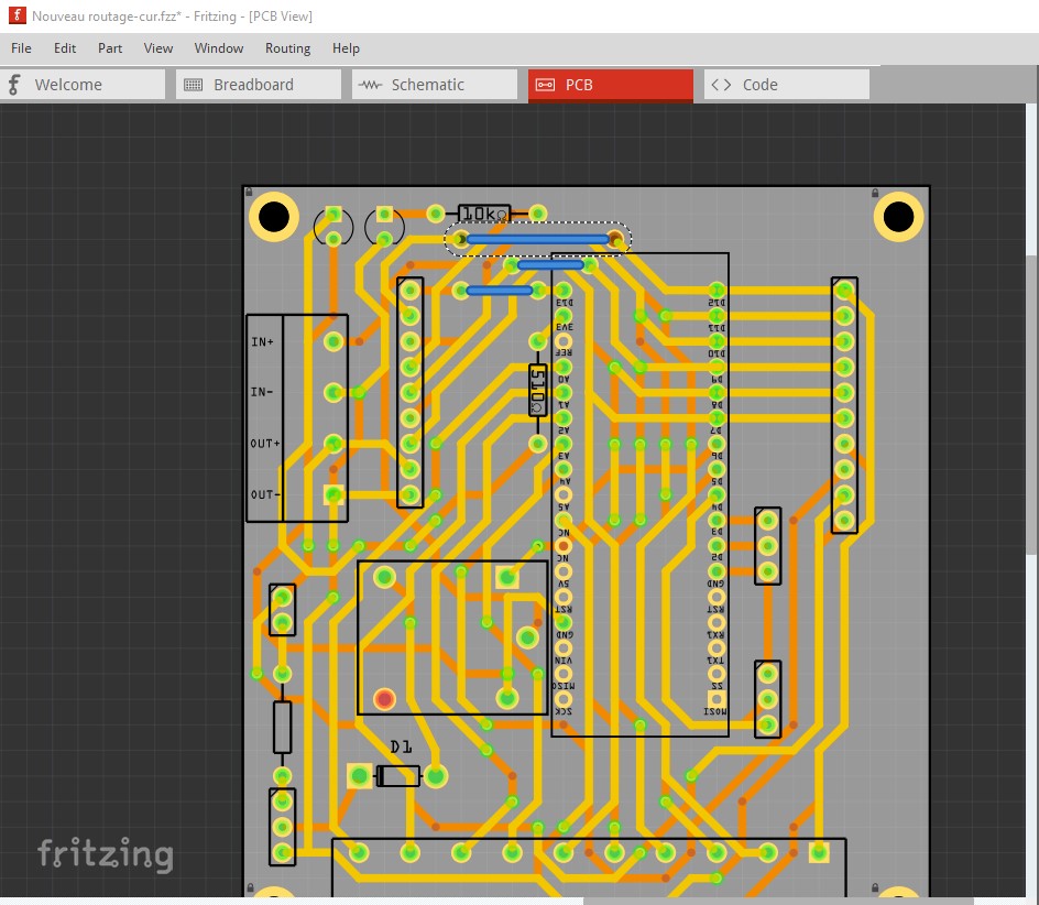
You are correct that in pcb this will work fine. In practice even though there are two pads on top of each other in pcb, what will appear on the actual board is a single pad and all will be well. The problem I fixed is that when the connection in pcb is reflected in to schematic, the jumper connection will be lost as Fritzing thinks the connections are to the two pads that don’t connect to each other (only the jumper has that connection and it isn’t connected to the pads.) Pictures hopefully will make this easier to understand. Here is your original pcb with the jumper moved out of the way and schematic routed.

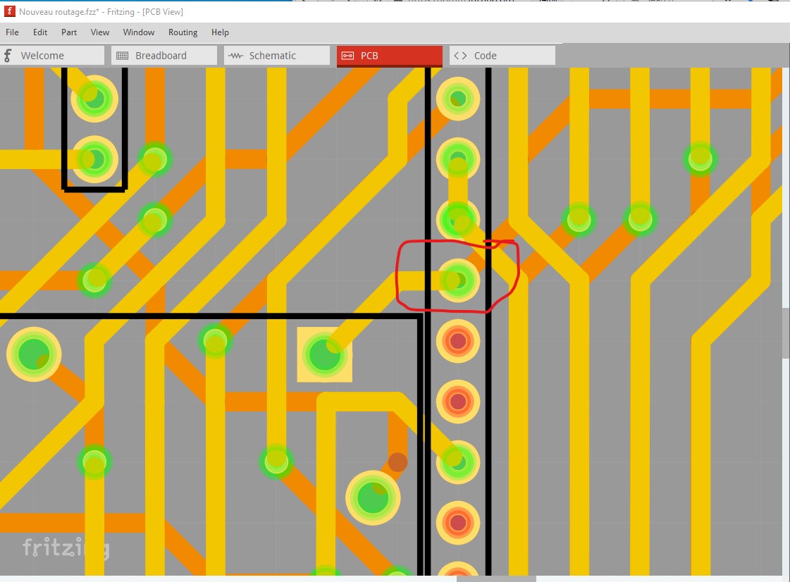
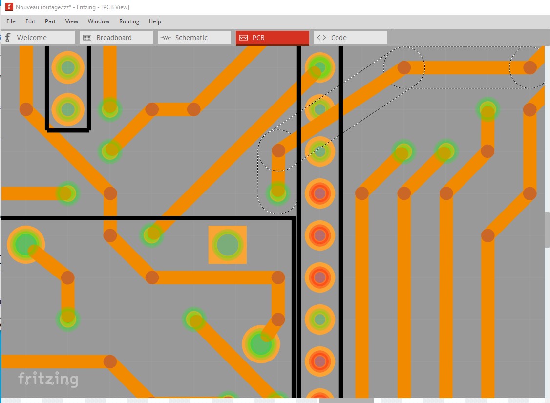
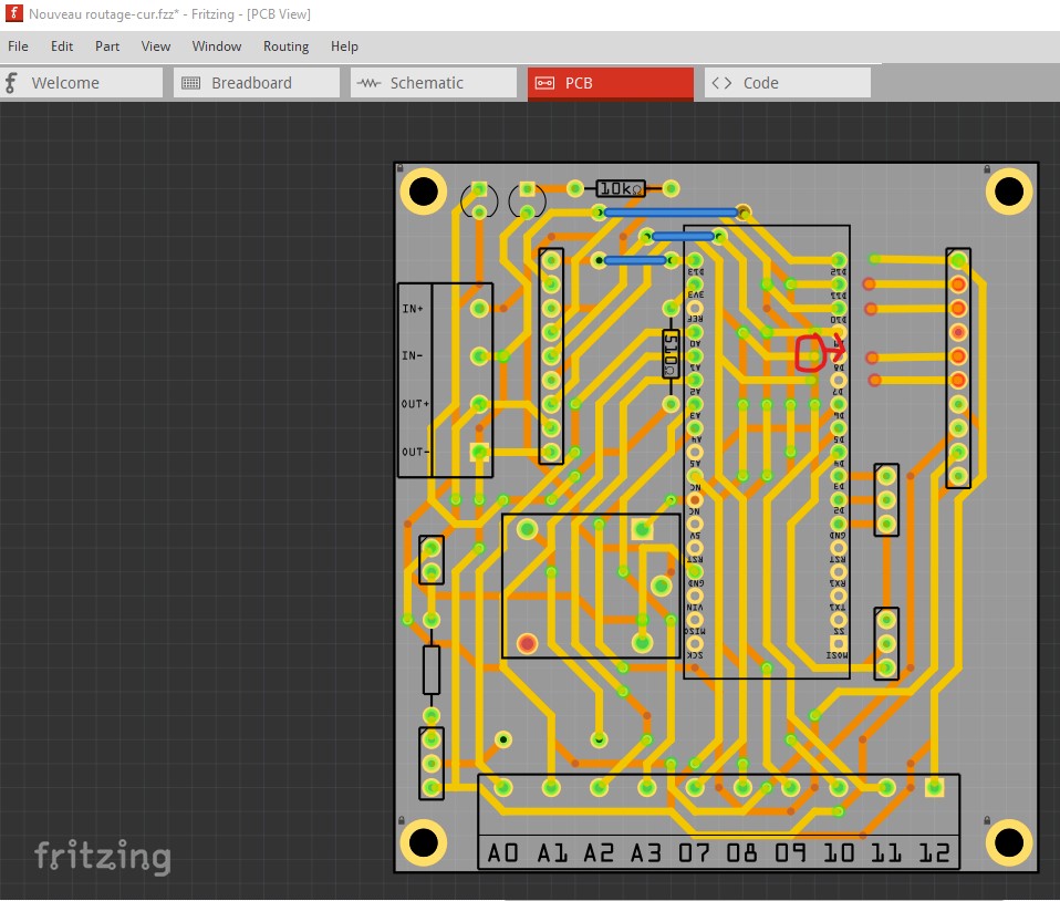
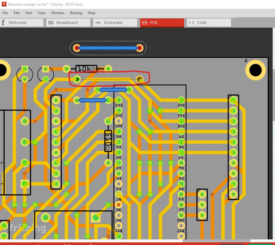
Note the rats nest line between the pads. This is there because there is a connection between J5 pin1, Micro D12 and J4 pin1 in schematic, but (because of the jumper not connecting to the pads under it) not here in pcb. If I switch to schematic

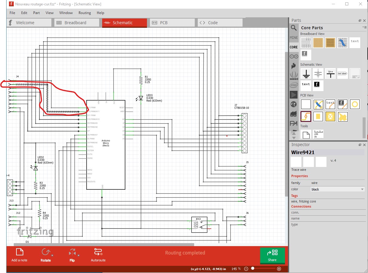
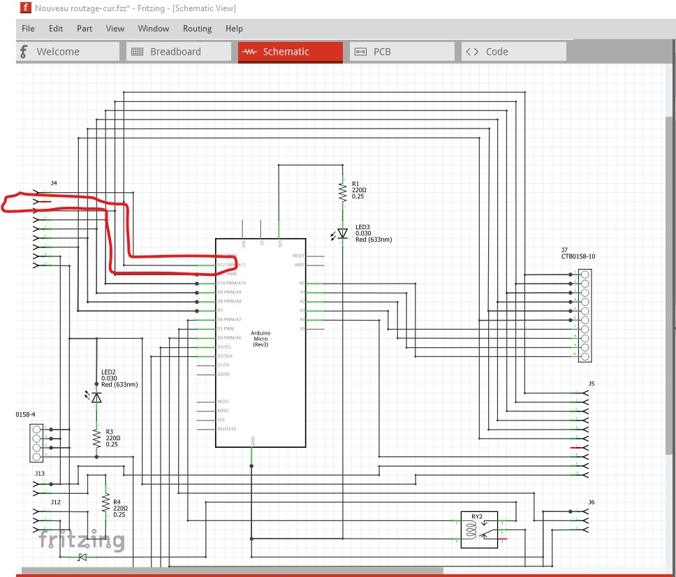
the rats nest in pcb view corresponds to this connection in schematic (outlined in red in the image above.) If I delete this connection in schematic, the rats nest line in pcb will disappear as Fritzing no longer knows the two pins should be connected.

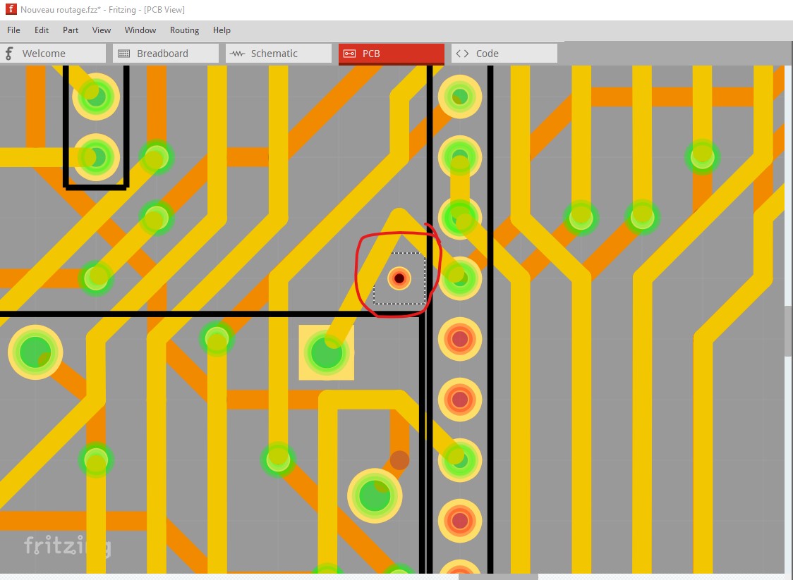
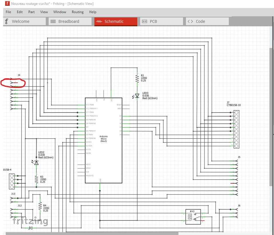
now pcb no longer shows the rats nest line

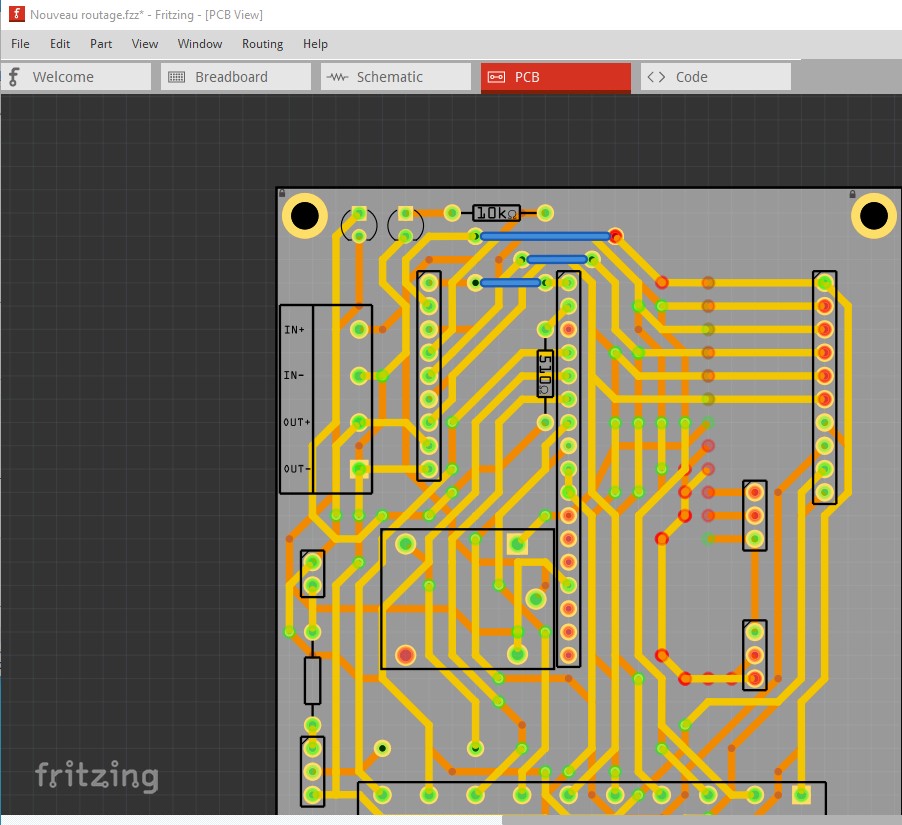
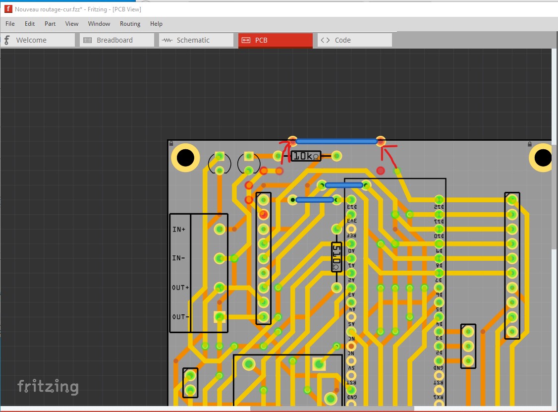
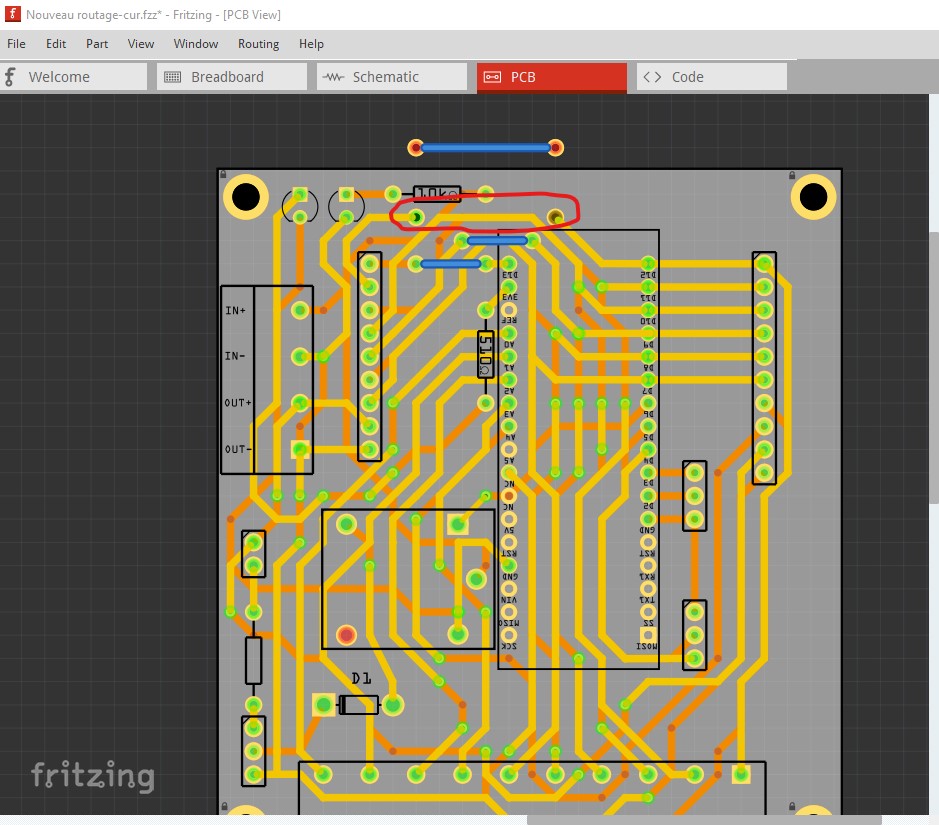
so now I move the jumper back on top of the pads as your original sketch was.

In pcb everything looks fine (and in fact will work fine, because the pads will exist and connecting a jumper between them will work) but in schematic things are not the same and Fritzing is not telling us that something is missing (because it doesn’t know anything is missing!)

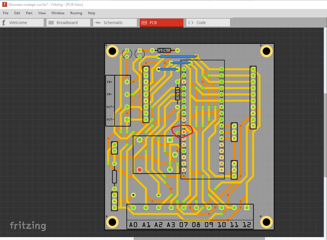
there should be a rats nest line going from J4 pin2 to Micro pin D12, but there isn’t because Fritzing isn’t seeing the jumper in pcb as connected, only the two not connected pads under the jumper like this. Here I changed to the sketch with the pads removed (and moved the jumper up to show the pads are not there)

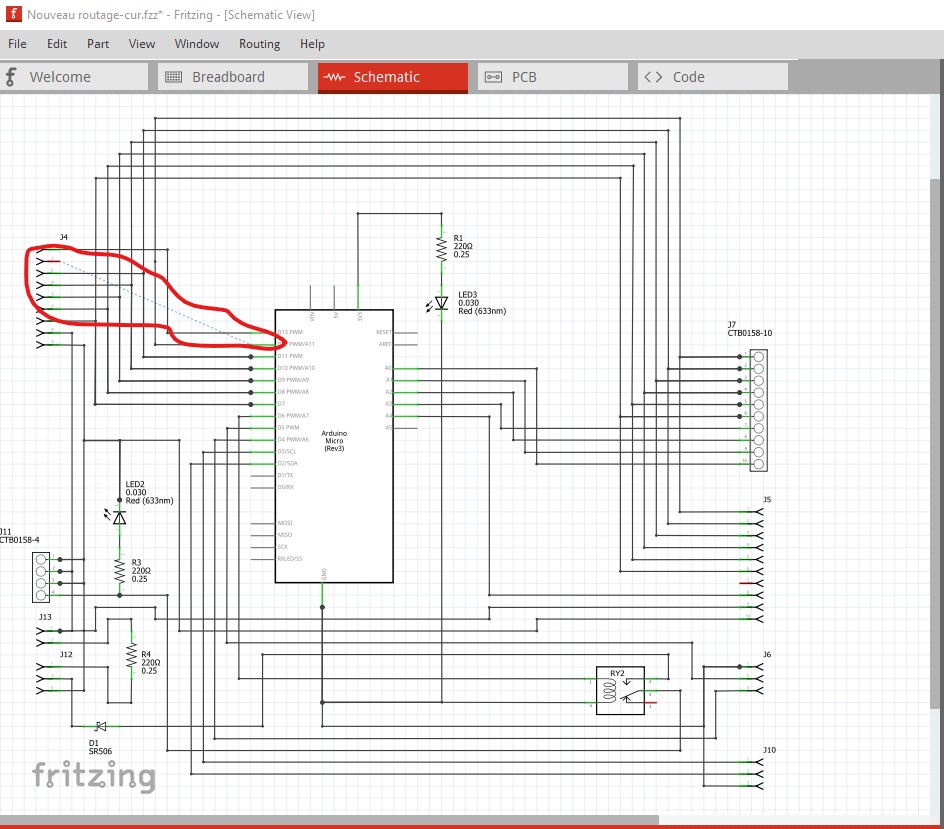
now if I delete that same wire in schematic, a rats nest line will appear to indicate there is a connection in pcb that is missing in schematic.

to indicate we have missed a connection. This allows me to cross check the routing in pcb with what I expect to be there in schematic which helps to discover missing connections (which are easy to make in a complex pcb!)

I don’t mind questions when you don’t understand. I have been doing electronics for more than 50 years now, and often assume things are common knowledge which are not common knowledge for a beginner. So a question usually means I have assumed knowledge I shouldn’t have.

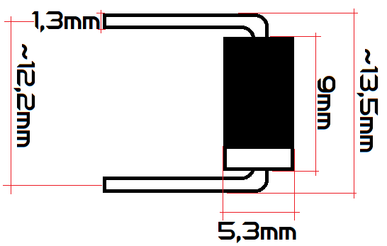
I hadn’t realized how big that diode is! I have updated the part so the spacing between pads is now 0.5in rather than the 0.3in it was. That should give sufficient room to fit it.

Yes something like a 1n4001 1A 50V rectifier diode should do fine. A small signal diode such as the 1n4148 probably doesn’t have enough current capacity to deal with the surge.

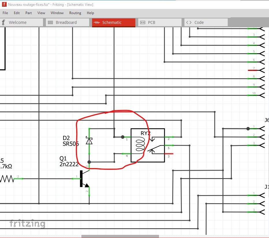
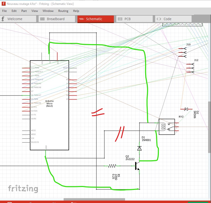
It isn’t. D2 connects across the coil of the relay, the emitter of the transistor is on ground. When the transistor shuts off, the coil of the relay will try and keep the current constant. The diode provides what amounts to a short circuit across the coil to dissipate the energy from the coil without damaging the micro with a voltage spike.

I assume this should be pin 1 of the relay? In your original circuit the relay was connected to a pin of the Micro and ground. When the I/O port was high the Micro provided 5V through the I/O pin to drive the relay. In my circuit the drive from the Micro is causing the transistor to conduct and pulling pin4 of the relay to ground. The relay now needs pin 1 connected to 5V on the Micro so when the transistor is on, there is 5V across the relay and it activates. The 5V from the I/O pin is now driving the transistor, so the relay needs a source of 5V to operate.

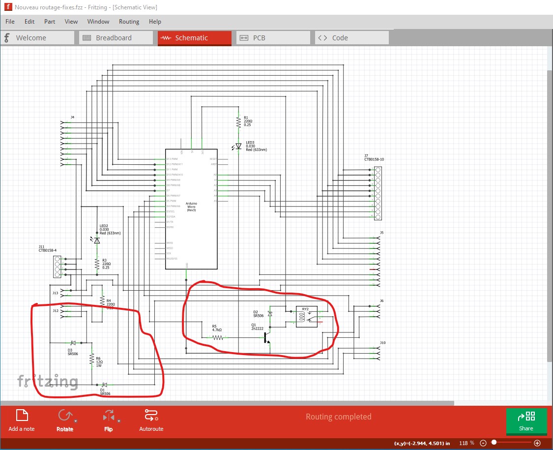
That is because there is an error in my sketch. Here is a corrected one

Nouveau routage-fixes.fzz (76.0 KB)

capture11

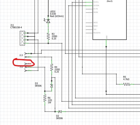
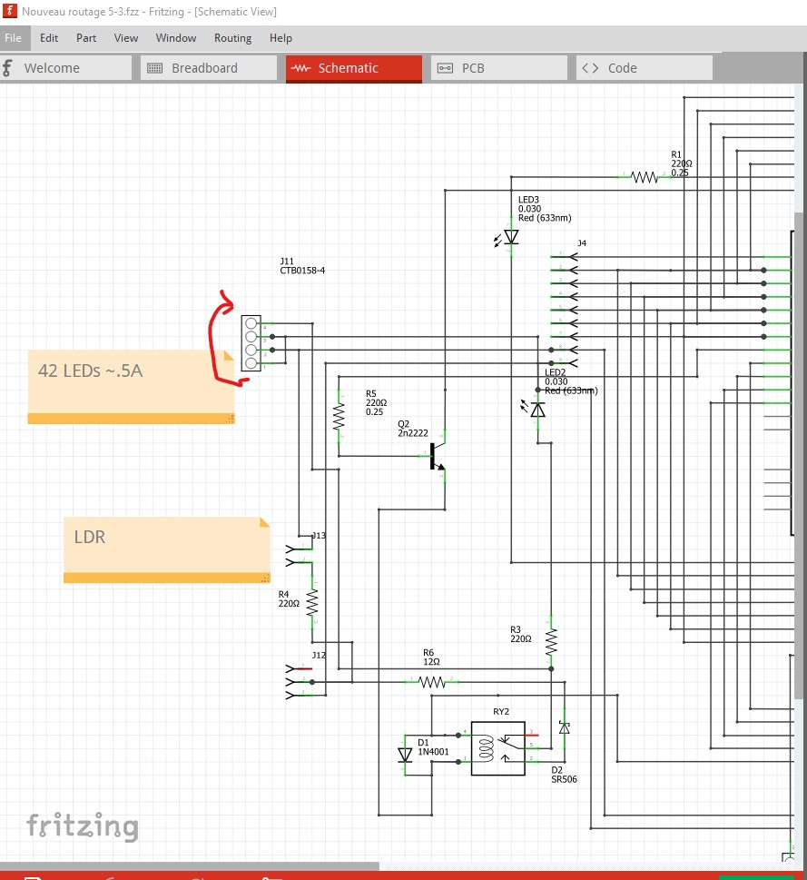
Pin 3 of J12 is disconnected because it is shorted to pin 2 on the capacitor board and thus isn’t needed. I substituted a 1n4001 across the relay coil and used the new version of the SR506 with wider spaced pads. Assuming the light sensor is a Light Dependent Resistor, unless you have found an unusually powerful one, this isn’t going to work (and even then the 220 ohm series resistor is a problem.) Assuming the 42 LEDs take 10ma each (20ma would be more usual!) that means they need 420ma which is likely much more than the LDR can handle. I expect what needs to happen is that the LDR output should go to the A5 pin on the Micro and one of the PWM pins should drive a power mosfet to dim the LEDs. I haven’t so far added that to the schematic, because I am not sure of what you are wanting to do here.

Peter

So I fixed some problems, installed the new components ect.

I understand that the second red wire is not necessary for operation but I will keep it anyway, I like it. : P

The pin that goes through the NC is a fault but that’s okay because I’ll replace the board with the headers and the error will go away.

The 4.7k resistor is too high but I’m still going to look at the 2n2222 datasheet to calculate the correct resistor ^^

Thank you once again.Nouveau routage 4.fzz (54.6 KB)

Maybe a little high, it creates a base current around 1ma ans with a gain of 100 that allows about 100ma of collector current, so perhaps a 2k2 resistor would be a better choice. That will provide about 2ma of base current and thus about 200ma of collector current which gives you more margin.

edit: As well the relay isn’t connected correctly. Here the double red slashes indicate a disconnection and the green indicates the correct connections.

the diode needs to connect across the coil and the coil top needs to go to 5V. As well the second sr506 and the surge limiting resistor to the capacitor bank are missing. The current connection won’t provide any surge limiting to the capacitors.

Peter

I do not understand exactly everything you are explaining to me, I changed the connection of the transistor because it worked but indeed it was connected backwards.

I did some test with the base of the transistor and 1k ohm is already preventing operation.

I’m sorry I’m taking a long time because my health prevents me from concentrating at the moment (nothing serious, just binding ^^)

By copying onto a breadboard what I did on the components view, there is no problem. So I don’t quite understand. The 5v passes through the 2n2222 then puts the relay coil under tension with the GND on the other side. I put a diode as you had advised to avoid the return of the coil when it goes to OFF so why remove it now?

Yes I have to put a Maasedqais resistance of how many ohms so that it does not go below 12v?

I am really sorry for my dificulties in understanding between my lack of knowledge and the approximative translation problems of our friend google ^^

Here is where I am.Nouveau routage 5.fzz (76.8 KB)

Nothing to be sorry for, reply when ever you can, I’m not in any hurry. The important part is for us to get something that will work for you!

It will indeed work as an emitter follower (which is what you have now) but a 1k resistor should give about 5ma of base current which should switch up to 1A or more at the emitter, so the relay should work with a 1K base resistor. The diode needs to go across the coil not in series with the coil. Here I have made the necessary changes in both schematic and pcb to produce a correct configuration.

I rotated the power connector by 180 degrees so it matches the orientation in pcb (input power at the top and gound at the bottom.) The diode is across the coil as it needs to be, I added a value (12 ohms will limit the charge current to about 1A) to R6 and moved the connection on J12 to pin 2 (as pin2 and pin3 are connected together on the capacitor board which will cause a loop which is undesirable.) Here is a copy of the complete sketch:

Nouveau routage 5-3.fzz (78.1 KB)

As I understand it there are 42 LEDs connected between pin 1 and pin 2 of J11. Assuming 10ma per LED that would need .42A to power them. R4 at 220ohms and the LDR on J13 won’t let 0.42A flow to the LEDs so I expect I am misunderstanding something here.

This appears to be a problem with translation. As it stands it doesn’t make any sense to me. Which resistor in the drawing are you interested in the value of?

Peter