Having tried many other schematic design apps I tried to use Fritzing to do the same.
I wasnt pleased with the results, even for a very simple circuit.
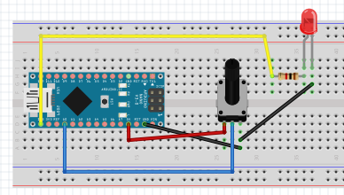
Sorry this will take a few replies as I can ony paste 1 image at a time.
Having tried many other schematic design apps I tried to use Fritzing to do the same.
I wasnt pleased with the results, even for a very simple circuit.
Sorry this will take a few replies as I can ony paste 1 image at a time.
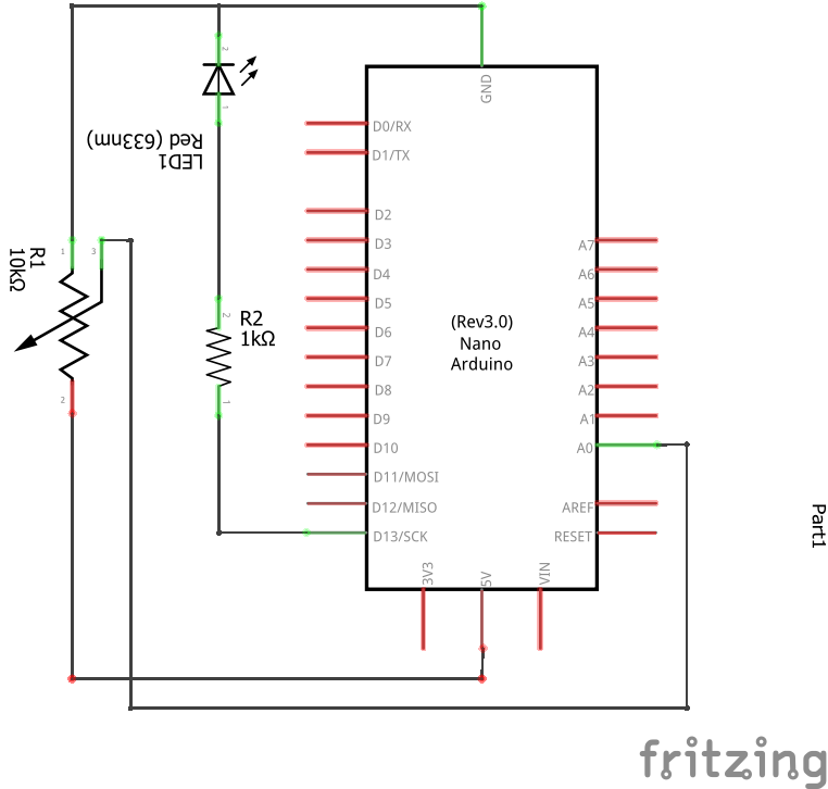
Here is the schematic Fritzing produced
You can see the power rails are not where they should be nor are inputs left and outputs right.
Am I just doing it wrong? I find the interface very idiosyncratic as compared to other schematic apps.
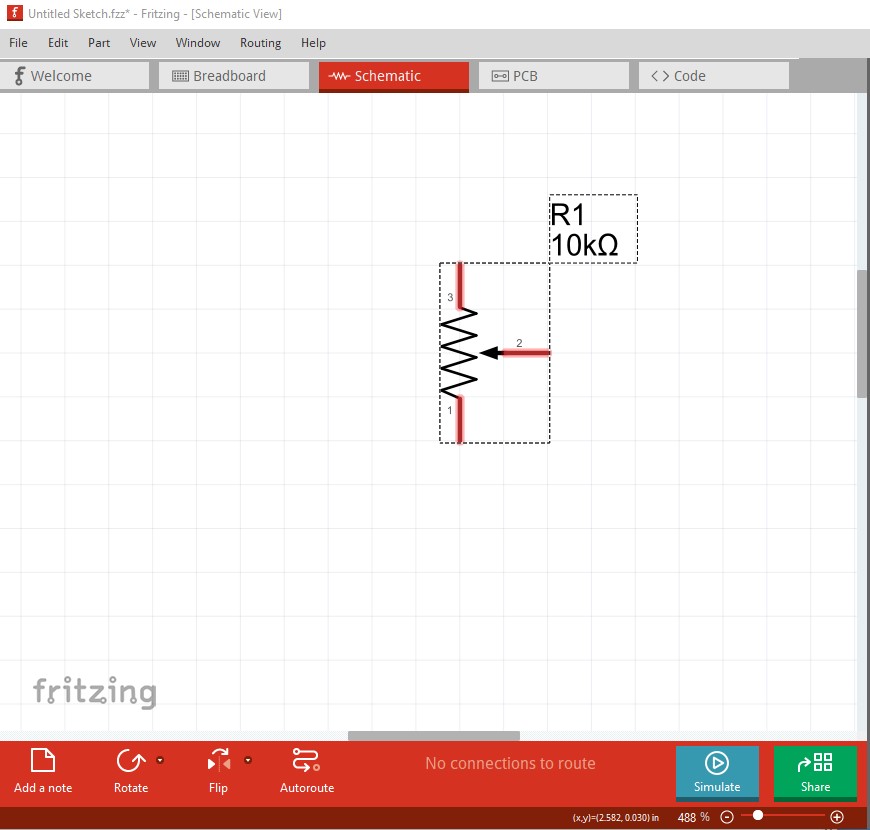
First, what fritzing version are you using (current is 1.0.0)?) I ask because the pot in your images is old style, the current versions look like this in schematic:
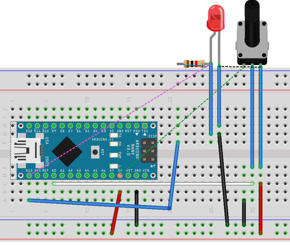
This part was recently updated from the original layout which is as you show in your images. Then unlike most other EDA packages Fritzing reflects changes in any view (such as schematic) in to the other 2 views. Sometimes this causes problems if there is already a conflicting connection in another view. That is possibly what happened to your breadboard image. This is a relevant topic because there is a discussion going on on github here
the intent of which is to update the standards docs to specify part and schematic specifications with the view to then updating the core parts to match the new specs. That however will likely take a long time even when the discussion completes (if it completes) as it is going slowly. The requirement for a “standard” schematic has come up, but I am unaware (which may just be my ignorance!) of a standard. Apparently Kicad has a standard of some kind but pointers to examples and/or desires for formats preferably with documentation would be desirable. Most of the parts in your images are old (more than 10 years) and development in Fritzing stopped in 2016 (and started again a few years ago) which means not much got changed for quite a few years and the standards have always been relatively incomplete (and changing them has been in the past controversial!) There is now a head developer who has the ultimate say in what gets done (in the past the discussion was among users because there were no developers!) That said you breadboard problem is likely solvable by deleting all traces in breadboard (Routing->select all wires, then delete) which will reduce the wires to rats nest lines sourced from schematic. As part of that there is currently a bug where changes made in more than one view can cause routing database corruption which ruins the entire sketch (and the only solution is usually to start over.) So the advise is make all your changes in one view and then click on (and correct if needed) the rats nest lines in the other views. After 5+ years of trying to reproduce this bug I finally managed it (and the developers found an even easier way to reproduce it!) and some fixes may have made it in to 1.0.0 but more are still needed. Til that is done the advise still stands (although it isn’t necessarily only changes in more than one view that causes the problem!) Hope this helps some!
Peter
Ignoring the pot graphic version and potential future changes, I have never seen changes done on schematic view cause parts on breadboard view to move. Did you move them yourself to show the wiring problems that resulted from the cleanup of the schematic view?
I “expect” that what happened, is that when cleaning up the schematic view, you connected to the opposite ends of the both the resistor and pot. Electrically that does not make any difference, but because Fritzing links wiring on all of the views together, it “added” those new connections to breadboard view. That is where the dashed “rats nest” wires in breadboard view are coming from. Indications of that, are the green rats nest wire from the pot to 5V on the Arduino, the black rats nest from the “+” side of the pot to the “GND” side of the LED, and the pink rats nest from the “wrong” end of the resistor to D13. There is also a rats nest wire from the other end of the resistor to the lead for the LED. All of this because your cleanup in schematic view “changed” which end wires are connected to. Your schematic image does not show it, but I expect rats nest wires there doing the same kinds of things, because, if the breadboard parts were moved back onto the breadboard, the wires there would go the opposite directions.
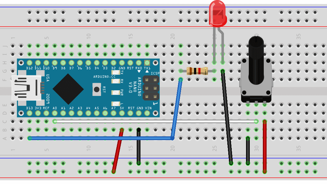
With Fritzing, the recommendation for best results is to do all of the wiring in a single view first, then route the rats nest wired created in other views, without creating new connections. Rotate and flip the components in that view to get the wires to route cleanly. If that is not enough, and you really need to change where the connection go (opposite ends of the pot), then go back to the original view, and change the wire connections there first. That will update the rats nest wires, and prevent the sort of issue you are seeing. In this case, rotating R2 in schematic 180 degrees and reverse the VCC and GND connections for the pot in breadboard view will probably get what you want. Instead of making any changes in breadboard view, in schematic, flip both R1 and R2 vertically.
For additional cleanup in schematic, I would replace the ground wires with 3 ground symbols, and the 5V wire with a pair of voltage bus symbols. But that is just my preference.
Thanks for your replies @microMerlin and @vanepp
I wasnt aware there was a new version of Fritzing, and when I looked at the download page I see no way to download it without paying - which I’m reluctant to do just to test it.
Maybe someone should update this on Wikipedia:
Fritzing is an open-source initiative[3] to develop amateur or hobby CAD software for the design of electronics hardware, intended to allow designers and artists to build more permanent circuits from prototypes. It was developed at the University of Applied Sciences Potsdam.[4] Fritzing is free software under the GPL 3.0 or later license,
uM
I’d agree with your analysis, I’ve played around with it a bit and my best result was starting from the schematic, then moving the components and placing the wires. IMHO thats a bit AAF compared to what a beginner would do.
Using seperate ground and voltage bus symbols makes sense in relation to the buses on the breadboard, less so on the schematic.
The reverse also works. Position and wire the breadboard, then do schematic. The condition there is to “use” the rats nest wires created in breadboard when working on the schematic. Re-orient the components on the schematic so that the routing will work, instead of creating a new wire to the opposite end of resistors and other components.
Using power and ground buses in schematic makes it much cleaner, once it gets a bit more complex. For the simplest cases, there is not a lot of benefit. For me, it is just ‘convention’.
EDIT: Fritzing is still open source software, if you have the time and skill to build it from source yourself. GPL is open “source” software. Executable apps are not included in that definition. Sometimes they are available for free as well, but it is not a requirement.