ich bin auf der Suche nach Printtrafos und kann mir irgendwie nicht vorstellen, dass ich der Erste bin, der Printtrafos auf seiner Platine aufbringen möchte. Jedenfalls habe ich nirgens etwas passendes gefunden. Daher wollte ich mal hören, ob es irgendwo eine Bibliothek mit Printtrafos gibt. Im speziellen suche ich diesen hier: El 48/16,8
Leider kenne ich mich überhaupt nicht aus mit dem Erstellen von Bauteilen und mir fehlt auch unibedingt die Zeit sich damit komplett von vorne zu beschäftigen. Das Tool eagle2fritzing ist mir zwar bekannt, die Installation funktioniert aber leider aktuell nicht bei mir.
Sofern mir jemand helfen kann sei Ihm schon mal ein großes Dankeschön ausgesprochen.
While this exact part doesn’t seem to exist, I made a couple of similar ones (except with dual secondaries) for someone 6 months ago. It is a relatively simple change from that to a part which should work for this. Before ordering boards print the pcb footprint at 1:1 scale and check it against a real part. The pin holes in this part are 0.038in (suitable for a .1 header connector), when the pin looks to be about 0.035in from the data sheet.
edit: The two primary pins are each 1.25mm to far from where they should be. Corrected in this new part:
Obwohl genau dieser Teil nicht zu existieren scheint, habe ich vor 6 Monaten ein paar ähnliche (außer mit doppelten Sekundärteilen) für jemanden gemacht. Es ist ein relativ einfacher Wechsel von diesem zu einem Teil, der dafür funktionieren sollte. Bevor Sie Boards bestellen, drucken Sie die Leiterplatte im Maßstab 1: 1 und vergleichen Sie sie mit einem Originalteil. Die Stiftlöcher in diesem Teil sind 0,038 Zoll (geeignet für einen 0,1-Header-Anschluss), wenn der Stift etwa 0,035 Zoll vom Datenblatt entfernt zu sein scheint.
Thanks a lot for your help.
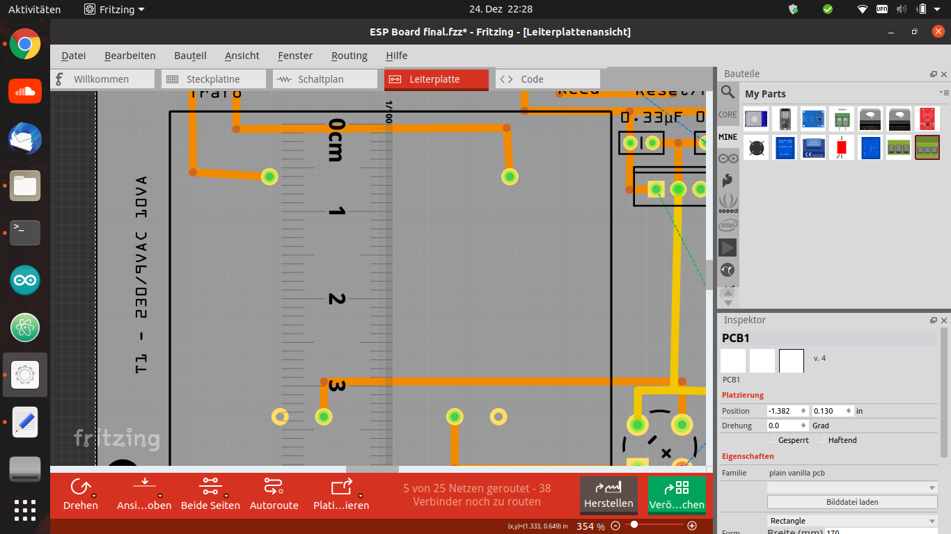
That looks pretty good, but on the 230V side the holes are each 1mm too far apart. They are not directly above those on the 9V side. I will add 2 pictures. The rest ist perfect. I’ve tested it with a footprint and the faulty pcb print. It would be nice if you could correct this one last thing.
Happy Christmas.
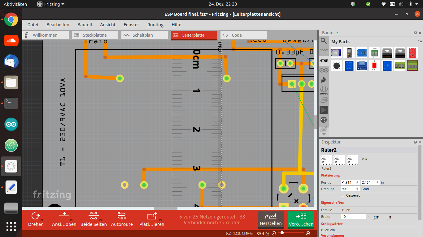
You are correct, I used the primary to secondary spacing value (27.5mm) rather than the correct 25mm so each pin will be 1.25mm too far out. As well because it isn’t clear in the documents whether there are pins in the two not connected pins on the secondary side I put pads with holes there in case the pins are there. If the pins aren’t there, then the extra pads can be removed if desired. I have replaced the part with a corrected version (at least I hope it is corrected !)