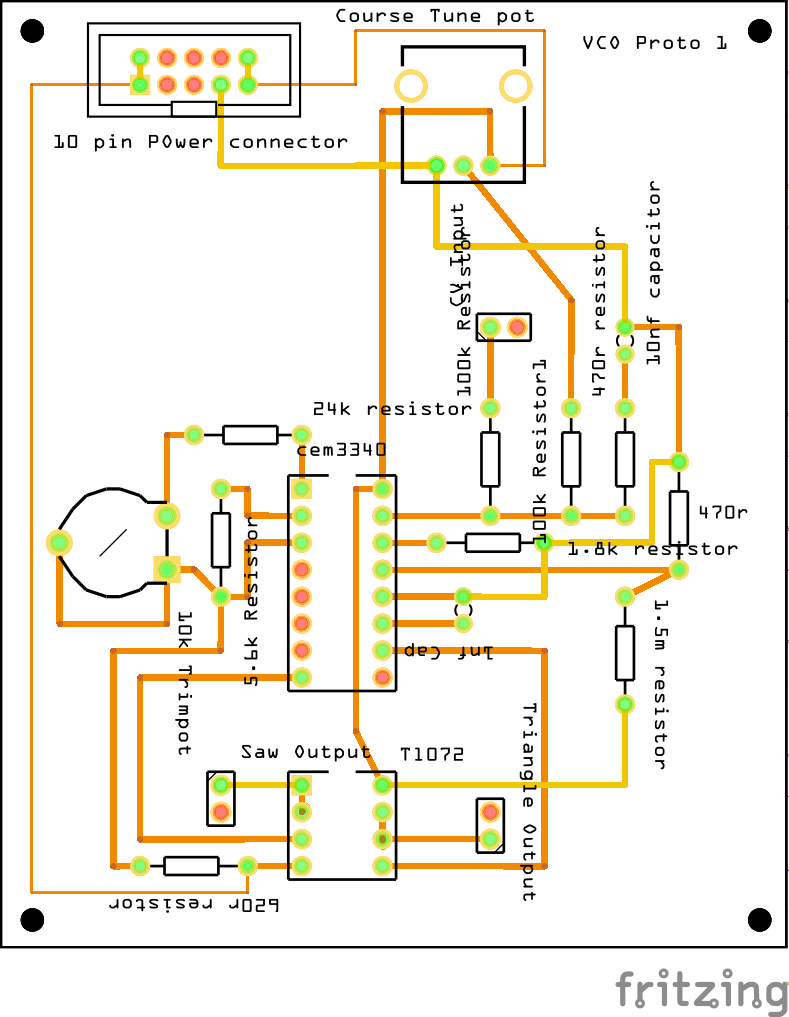
A quick look says the pcb wiring matches the schematic.
Using different trace widths in different places is fine (ground and power are often thicker than data lines, but there is no reason to go to the “super fine” 8 mil for the 2 bottom layer traces coming off of the power connector.
In general, shallow corner are preferred to the 90 degree used for most of that circuit. Shorter traces, and fewer corners are also generally preferred. A little work can cut some of those trace to half the length you used. Once the actual parts are positioned where you want (which optionally can then be locked to prevent accidental shifts), on a 0.1 inch grid, you can change the grid size to a smaller value, to help route the traces where you want.
‘backtracking’ traces is generally to be avoided. When practical, connect to the nearest pin for the net, then continue on to the next. Instead of going past, then coming back.
If you a planning to have that pcb created, cleanup up the silkscreen labeling would make it easier to used. Get the labels the right way up, and not over lapping on top of each other. Also for the labeling, you have control of the the content that is shown. Click a part shows in in Inspector (if that is turned on). The label can be edited. Click a part then right click the label has a menu option for ‘Display values’. Resistors for example have a resistance value. They are typically given label value of R0, R1, etc., and shown on the pcb as some combination or that label and/or the resistance. Other properties can be included in the label when desired.
Position any labels so that it is obvious which part it is associated with. Then labels are to long to fit, especially multi-work labels, shorten them, then add a second line using a text part (near bottom of the core bin parts)
You say that input and output connections will be grounded through the jack cases. It is not good to rely on that. Can you be SURE that the jacks are all connected together, so that the ground really always gets back to the circuit board?
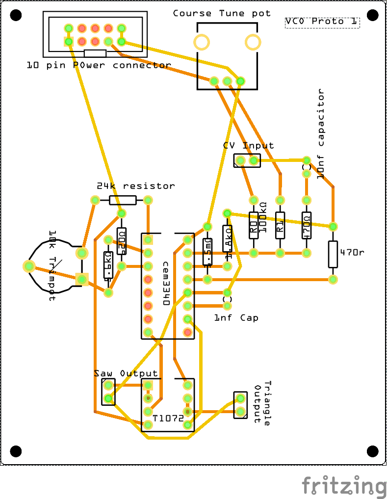
Small repositioning of a few components can make the routing cleaner. Here is an export of the pcb image from your sketch, and a version with some of that implement. Not complete, not optimized, but should give some ideas on what can be done.
And the modified sketch file to go with that, so you can check the property values and individual part label configurations.
VCO fritz file.fzz (24.1 KB)