Please look at my fzz file

Hi everybody,

would you please look at my PCB design and tell me if I can get it manufactured like this?

Unterstand_post.fzz (435.1 KB)

This board is supposed to hold

  • 1x Wemos D1 Mini
  • 2x MCP23017 I²C GPIO Expander
  • Terminal connectors for sensors/actors

I have not used the parts I want to connect as native fritzing parts (for example, there is a BMP280 part, but instead I used 2x screw terminal simply because those components are not supposed to be directly on the board, but rather connected via wires with some distance to the board itself.

These are the terminal connectors I am planning to use

I mostly used autoroute for the PCB itself, there was only one single component that I had to manually route.

The way I checked it, everything should work as expected. However, I am a beginner and this is very hard to debug for me. As long as nothing will create a short, I believe I got things wired correctly:

  • MCP23017 (addr 0x20) >>> D1 (SCL > D5, SDA > D4), and 5V/GND
  • MCP23017 (addr 0x21) >>> D1 (SCL > D5, SDA > D4), and 5V/GND, also A1 to GND (to change the address)
  • All components requiring 5V connected to external power source
  • All components wired to i²c GPIO expansion boards correctly (?)
  • ONLY the two REED sensors have GND, 5V, and DATA, even though though should only require GND and DATA (I did this so I could easily use something else in their place for another project without missing 5V)

I added the FREE terminal connectors for the same reason. While I only need one single PCB for my project, it’ll cost me almost nothing extra to order 20 pieces. So I thought I’d use one PCB without utilizing these FREE connections, but I’ll be able to use the same PCB for other projects and already have some VCC, GND, and GPIOs ready to use. (My original PCB design had another FREE connector for the GPIOs next in between MCP 0x21 and [FREE], but it was impossible to route, so I removed it. As it is very likely that other projects will not require 2x8 GPIOs to connect relays, I’ll be able to use those GPIOs as well.

Thank you in advance for your input :slight_smile: I had previously already ordered one batch of PCBs and something had gone wrong, so I am trying to make extra sure that this time I’ll actually be able to use the part :smiley:

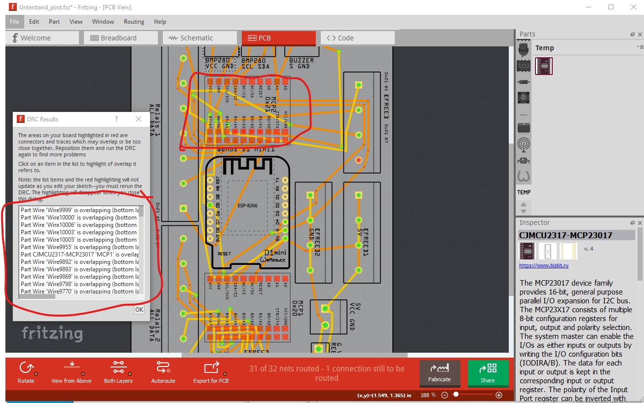
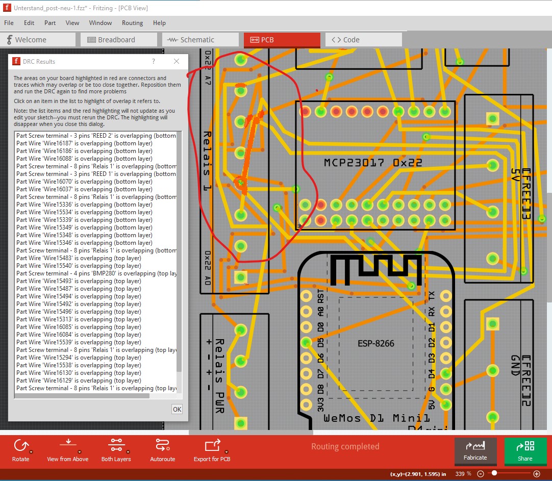
Right off the top the board doesn’t pass DRC (Routing->Design Rules Check) because the CJMCU2317-MCP23017 part is incorrectly configured (it has no copper1 layer) and as a result the traces are shorting the pins.

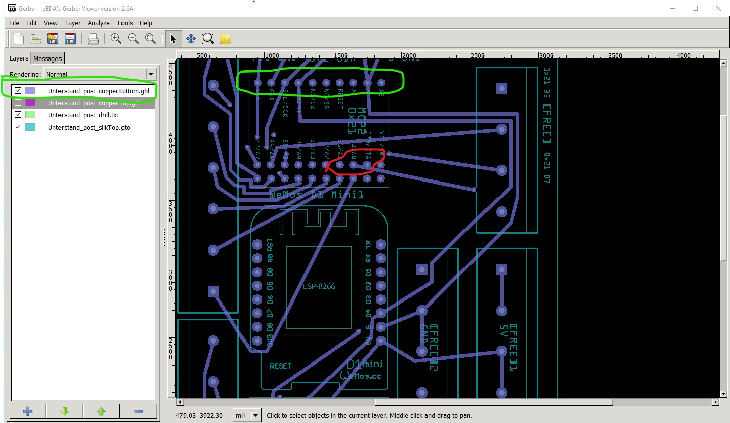
Here is copper0 (the bottom layer) as gerber output displayed with gerbv:

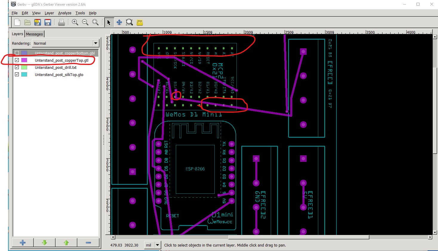
note the CJMCU2317-MCP23017 has pads on the bottom layer. But one of the traces is shorting the pin next to it (likely because the part is misconfigured) and when I display the top layer (which should have pads in the same place) there are no pads and thus no plating through on the holes:

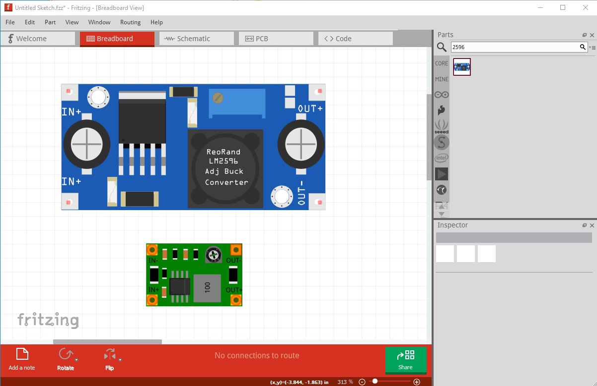
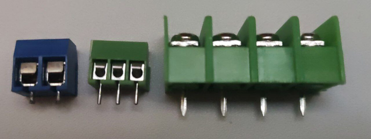
As well a number of the traces run through holes which will cause the trace to be destroyed due to the hole. I’ll fix the problems in the part and post a corrected one in a bit. After that we will need the data sheets (or at least the diameter of the pins in to the pcb) for the various connectors in the picture above to make sure the holes in the pcb are large enough to fit the pins. The hole size in Fritzing will be set to match whatever part the connector is designed for, if your parts are different the holes may be either to large (which is usually all right) or too small (which won’t work and makes the board unusable.) Then we get in to the issue of relays on the output pins of the CJMCU2317-MCP23017. It is very likely that the CJMCU2317-MCP23017 will not directly drive relays. It probably doesn’t have enough current drive to do so and likely lacks snubbing diodes to suppress back EMF from the relay coils. We would need the data sheet for the relays you intend to use to suggest a suitable driver circuit for the relays (you will likely need to add a relay driver chip to get enough current drive and back EMF protection.) The MCP23017 chip in the module will only source or sink 20ma of current which is not enough to drive most relay coils (and will likely be killed by back EMF without suppression diodes as well!)

edit:

OK here is a corrected part for the CJMCU2317-MCP23017.

CJMCU2317-MCP23017-fixed.fzpz (187.5 KB)

I changed its files and moduleId so it will load beside the original part. I would right click on the part and select delete which will delete both the part and all traces connected to it. I would then in pcb view do Routing->select all traces and then press the delete key to delete all traces and either manually route the traces (which gives the best results) or re run autorouter (which doesn’t work very well!) That should fix the trace issue and DRC. For your relays you likely need to add a uln2003A relay driver (available in core parts, do a parts search for uln2003 like this:

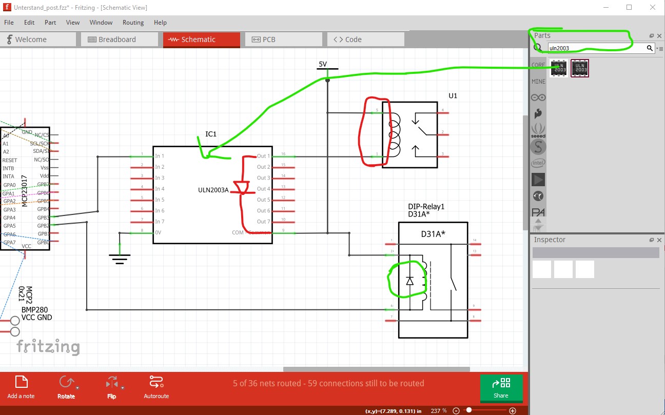
Here I have dragged the ln2003 and a couple of relays in to schematic.
The top relay has no diode across the coil (and may be high current, the 2003 will sink up to 500ma on each pin to a max of 2.5A for all pins.) The reed relay below it (which may be what you are using) already has the diode across the coil and is likely low current (although you would need to check that it doesn’t draw more than the 20ma the MCP23017 can sink!) and you can connect it directly to the CJMCU2317-MCP23017. If it draws more than 20ma you probably need the uln2003 relay driver. You would also need to check that the power supply (coming from the WeMos?) can provide that much current. All that remains is to determine if the pins on the terminal blocks will fit in the holes that are being drilled in pcb (and I don’t have the sizes of the pins on the terminal blocks!)

edit2:

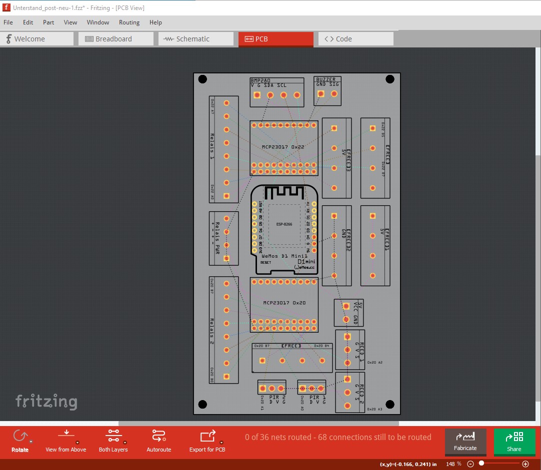
I decided to add the new part to the sketch, and clean up breadboard some. The start of that is to route schematic to make sure I don’t break anything. That turned up several current errors. In PCB there is one net not routed (but the current part makes it not routable, so fix it when the part is replaced!)

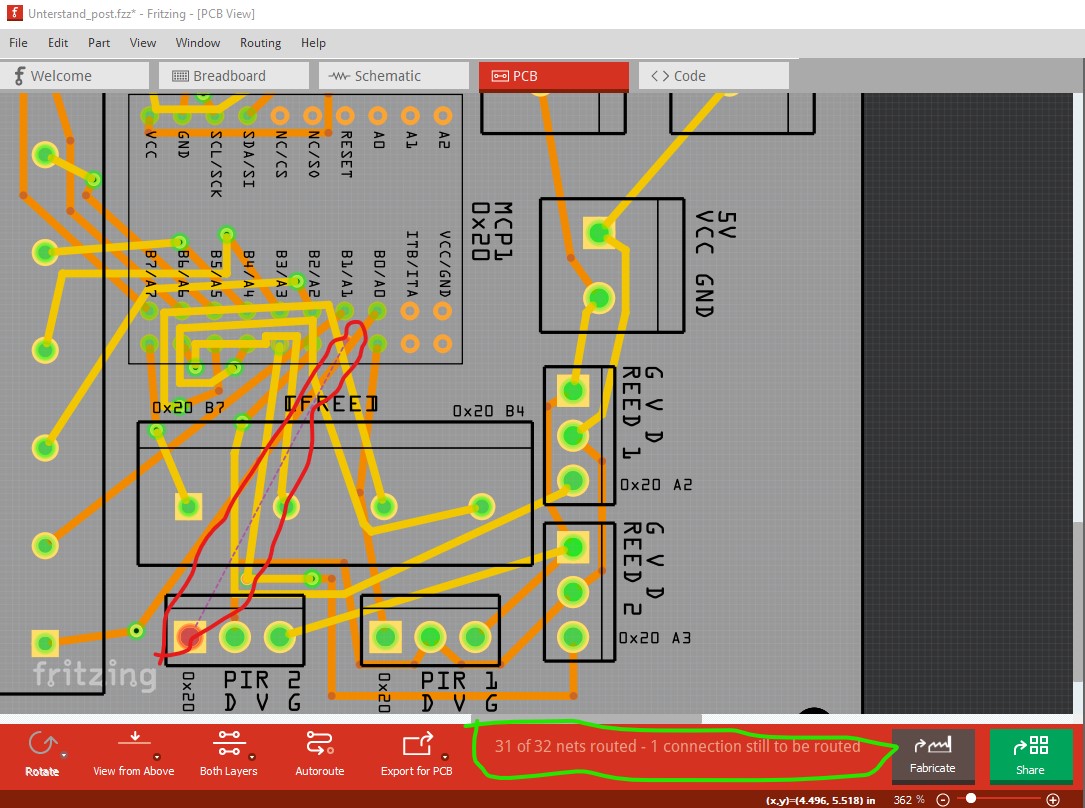
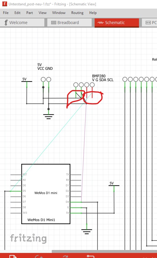
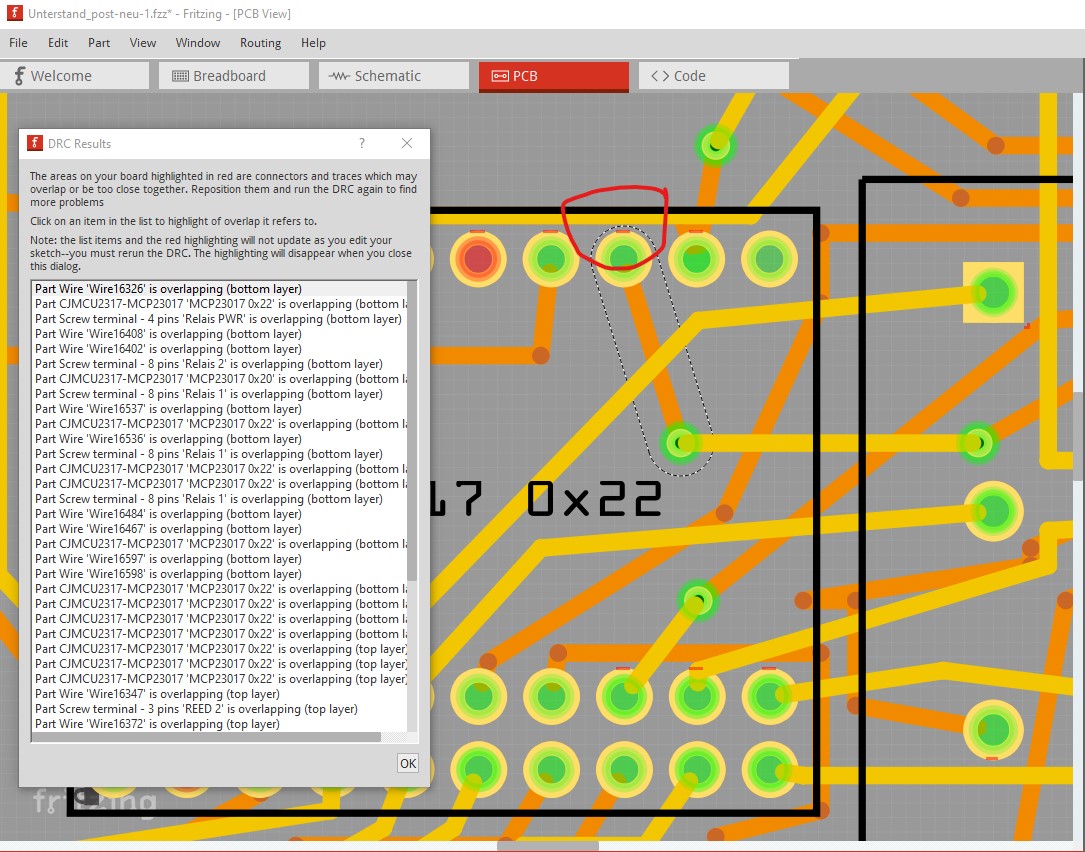
Note the bottom (circled in green) says 31 of 32 nets routed. That is indicating the rats nest line (circled in red) needs to be routed but can’t be at present because there isn’t a clear path to route it. Then when I routed schematic I noticed a couple of missing connections in breadboard:

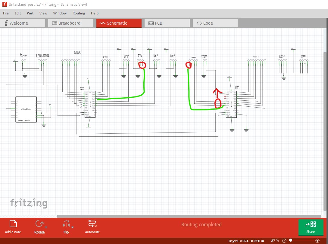
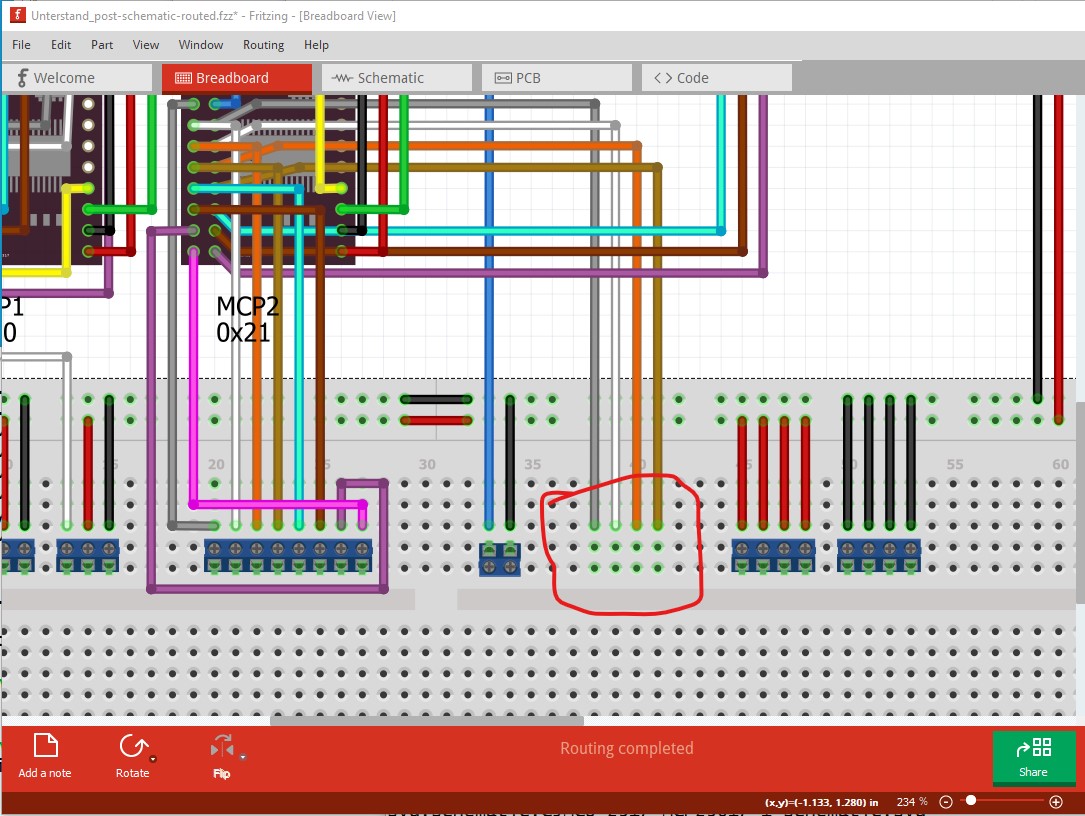
Note the data wire for reed2 is not connected to anything (I assume it should connect to the GPIO port with the green line.) As well one of the free GPIO part connections has no connection. I assume you want to move the first three up one pin and add a wire to the fourth pin as shown in green. With schematic now done I can go back and clean up breadboard some. Here is the sketch with schematic routed. Note the slanted wires on the MCP23017 are corrected in the new part which isn’t replaced in this sketch.

Unterstand_post-schematic-routed.fzz (453.3 KB)

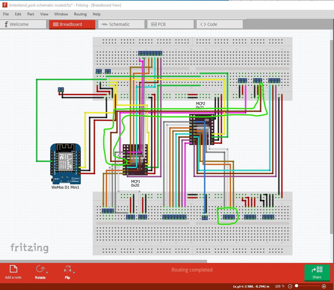
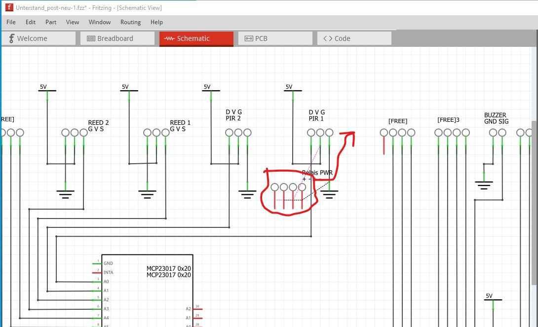
It appears there is a terminal block missing in breadboard which should be using those unused ports on the MCP23017. It of course is also missing on pcb …

edit3:

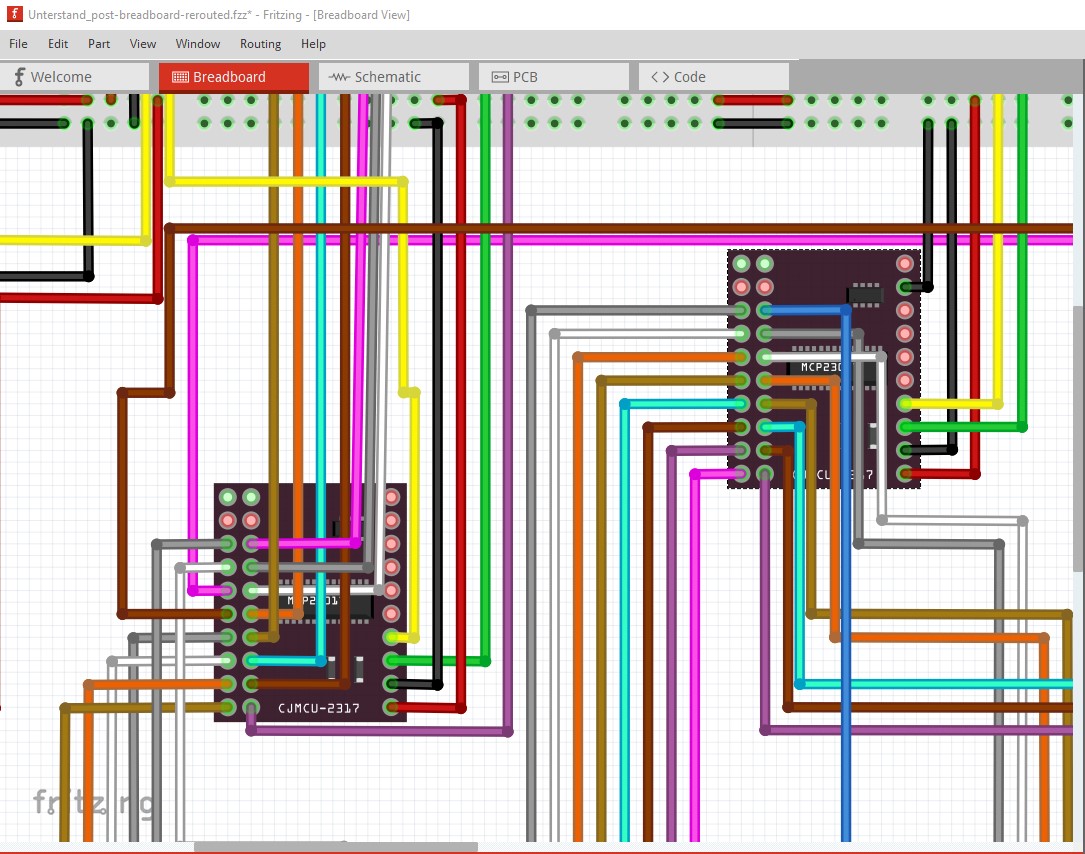
This time I rearranged breadboard by moving parts around to clean up the routing like this:

I added in the missing terminal block for the 4 free GPIO ports (and routed them in schematic and positioned the terminal block in pcb) and added in the missing wire for pir2 (I am assuming you wanted both of those done, if not you will need to remove them!) I then deleted all traces in pcb so nothing is routed there which results in this sketch:

Unterstand_post-breadboard-rerouted.fzz (437.0 KB)

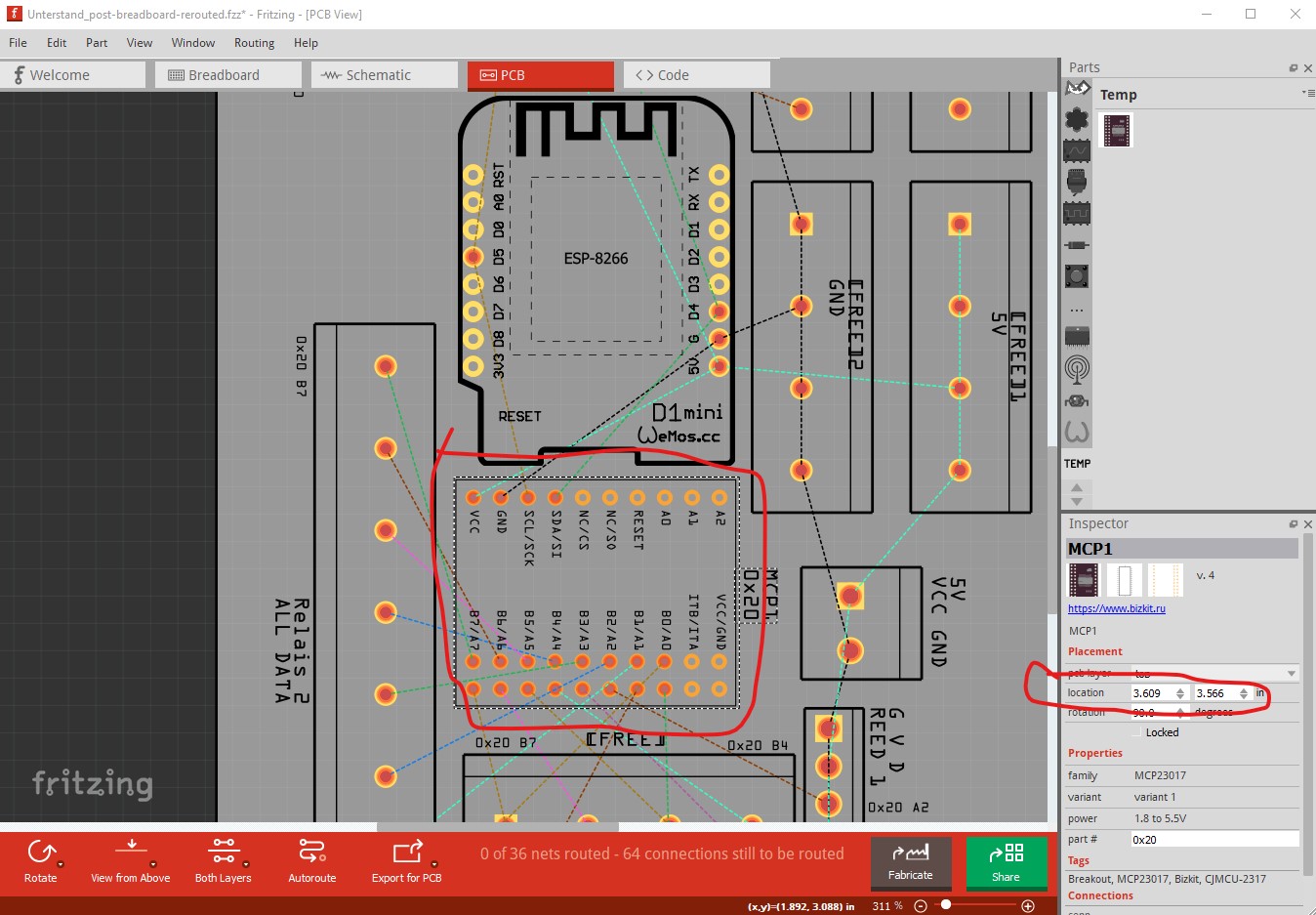
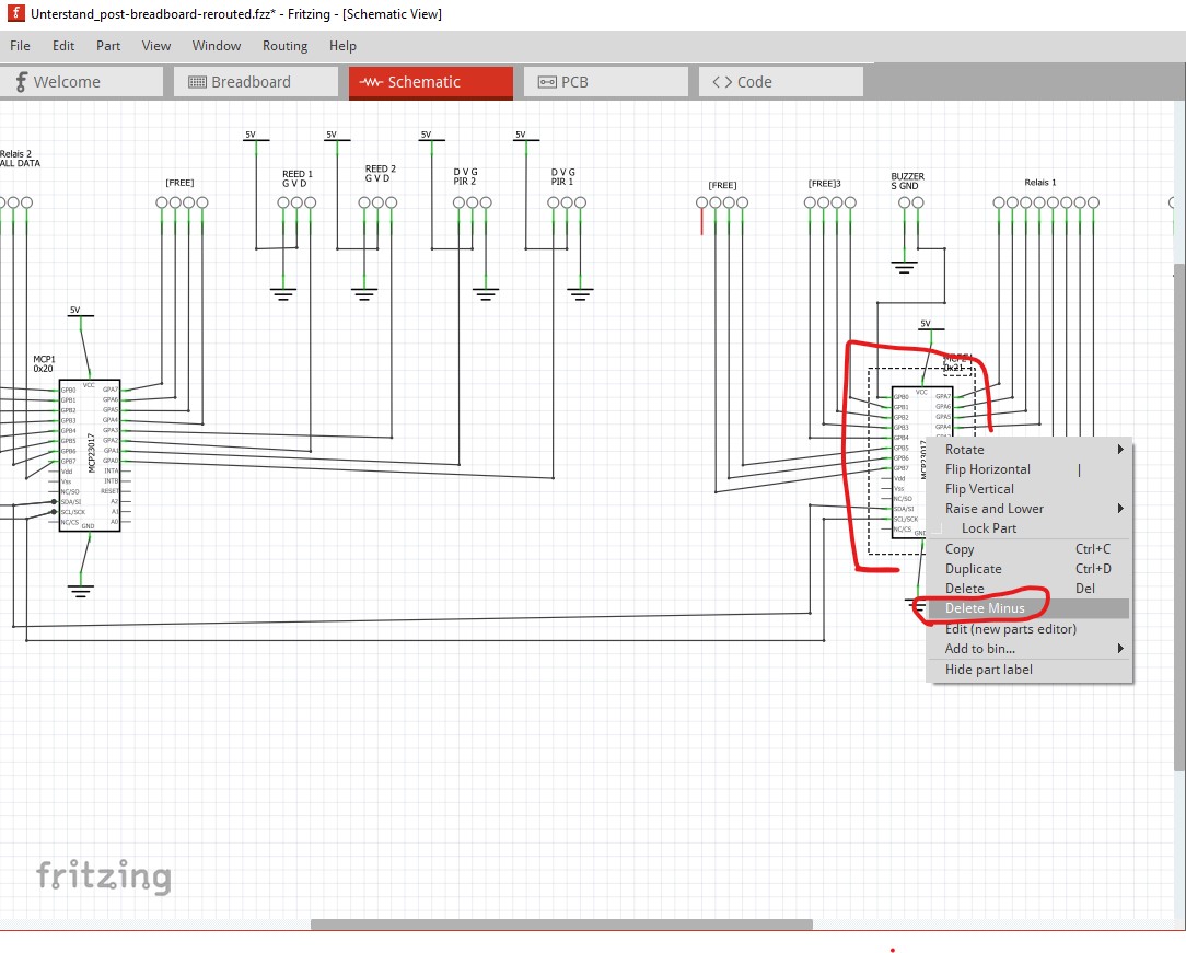
with that done I can now replace the 2 CJMCU2317-MCP23017 parts via delete minus. First I record the current coordinates of the 2 CJMCU2317-MCP23017 parts like this:

Then I delete the 2 CJMCU2317-MCP23017 parts via delete minus.

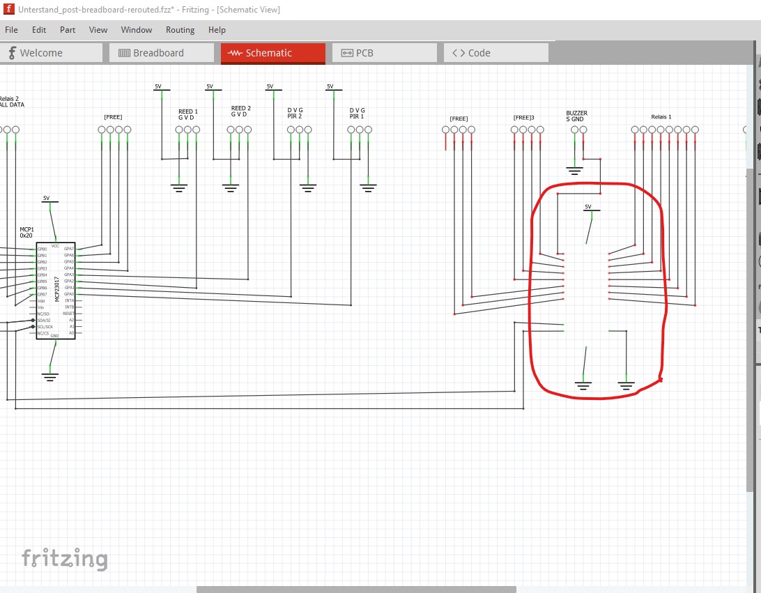
which results in this (the part is deleted but the traces are left in both schematic and breadboard)

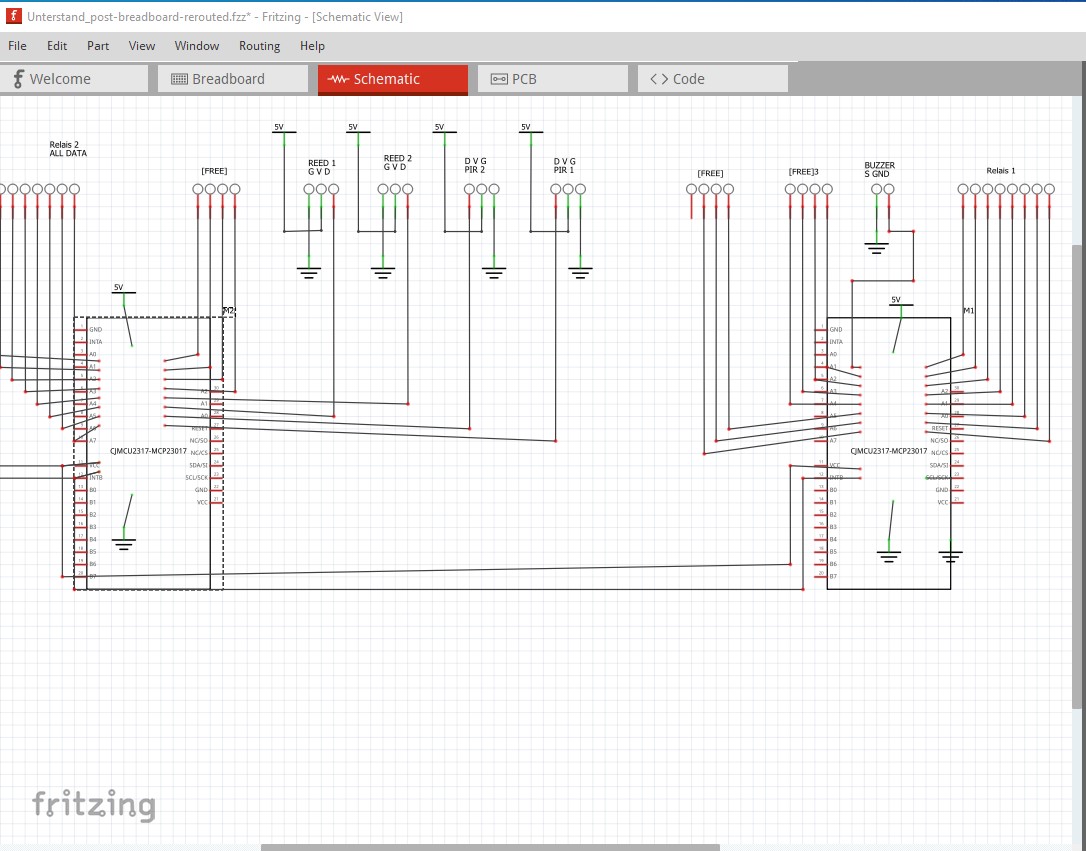
then I replace both parts with the new version. In schematic that is going to cause a fair bit of rerouting because schematic is much larger in the new part and the position of the power and ground pins has changed.

breadboard is the same size, so it will be easier

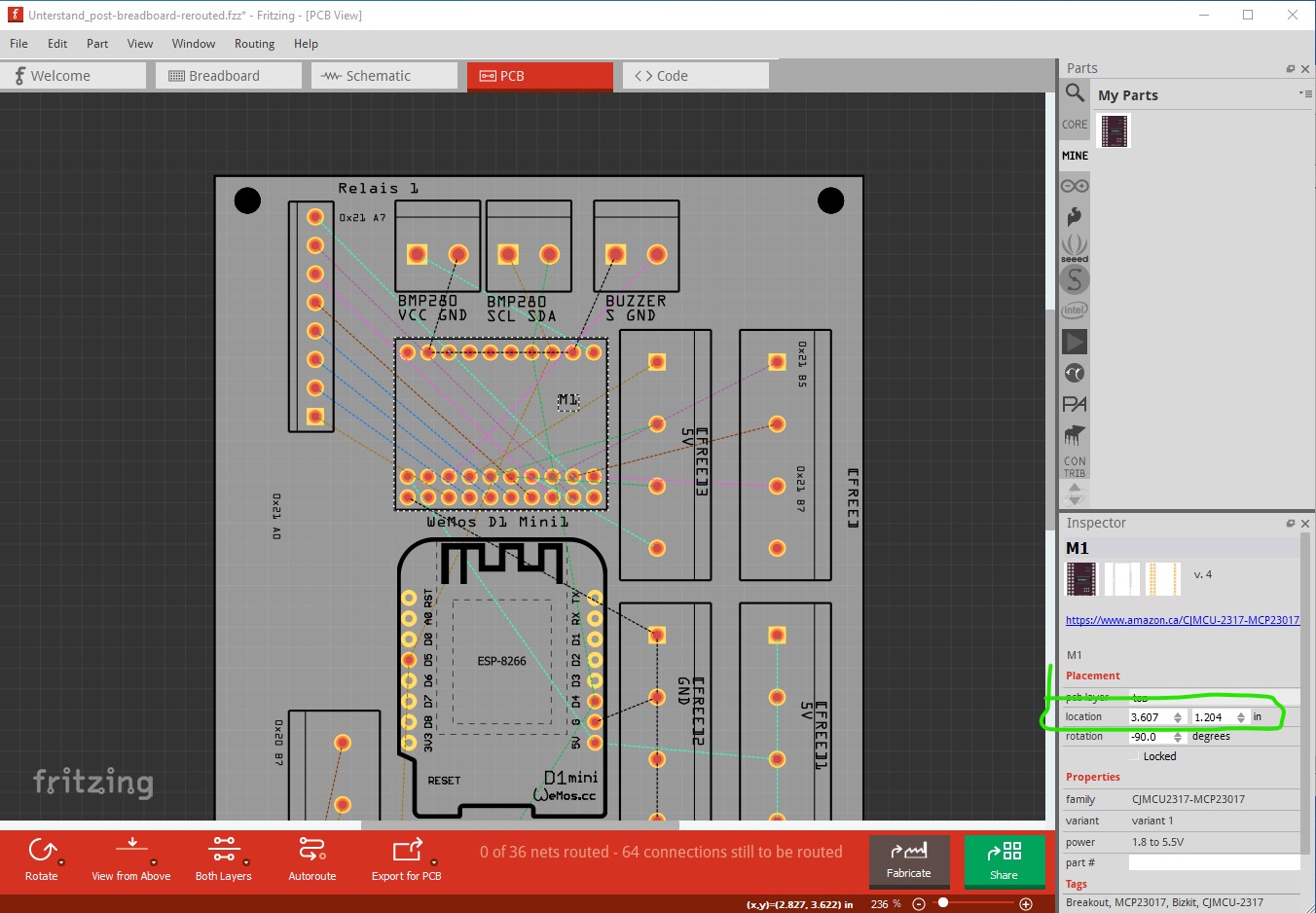
and indeed moving the parts in caused all the connections to reform and all appears well. Now I need to position the parts in pcb back to their original position using the coordinates we recorded above. In pcb the parts appear in a random position and orientation, so we need to rotate them til they are in the original orientation then use Inspector to move them back to the original position like this:

It is in the correct orientation but not the correct position, so set the x and y coords from the image that we took of the original parts above to move it back to the correct position.

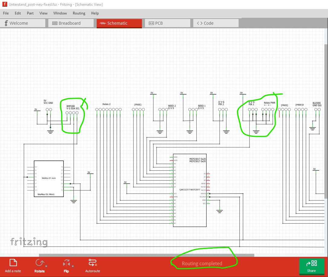
Note that the new part does not have the labels on silkscreen in the part. If you want those labels you need to use the pcb text part to add the labels yourself. The part is now back in the same place it started in, so do the same to the other one then move back to schematic to fix it up.

now both CJMCU2317-MCP23017 parts are in their original positions. Note the added terminal block that was missing in breadboard (circled in green) as noted if you don’t want this you can delete it. Now back to schematic to route the traces to their correct positions. In the end it turned out to be easier to delete all the original traces and reroute schematic from the rats nest lines producing this:

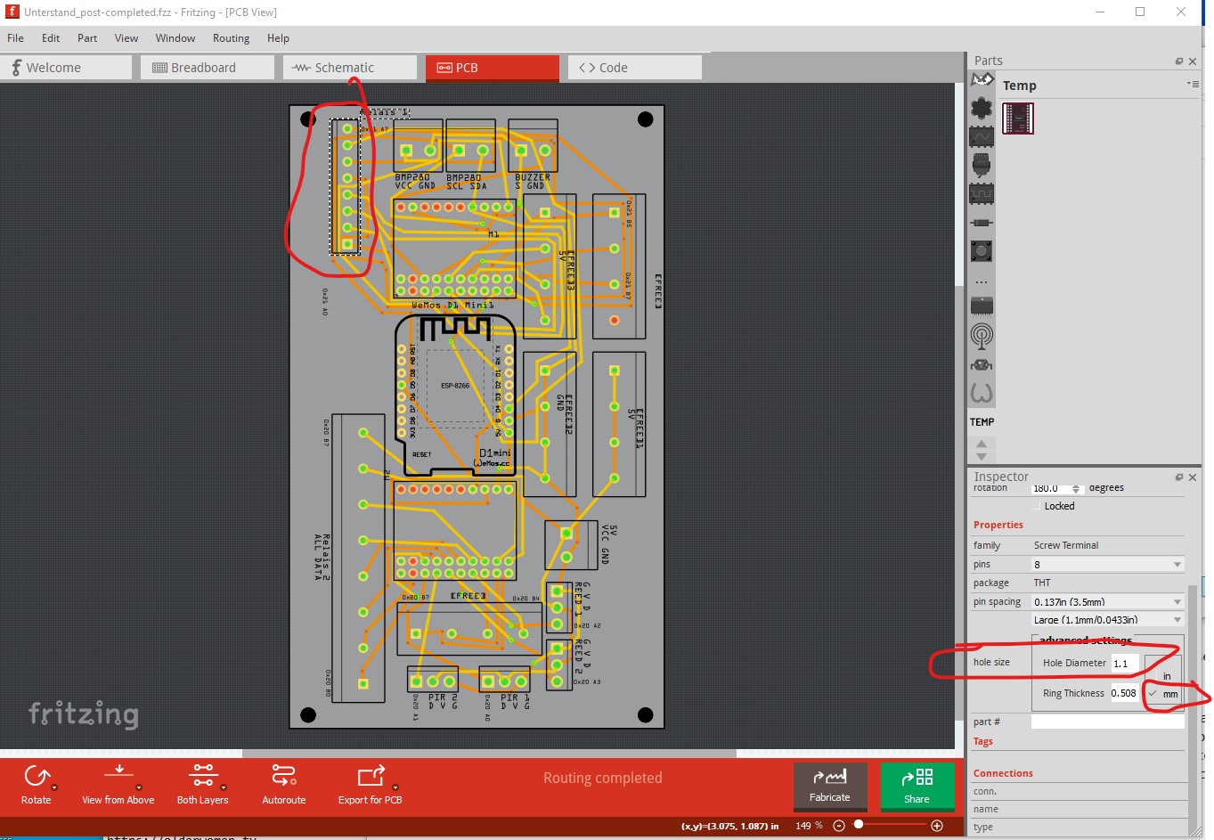
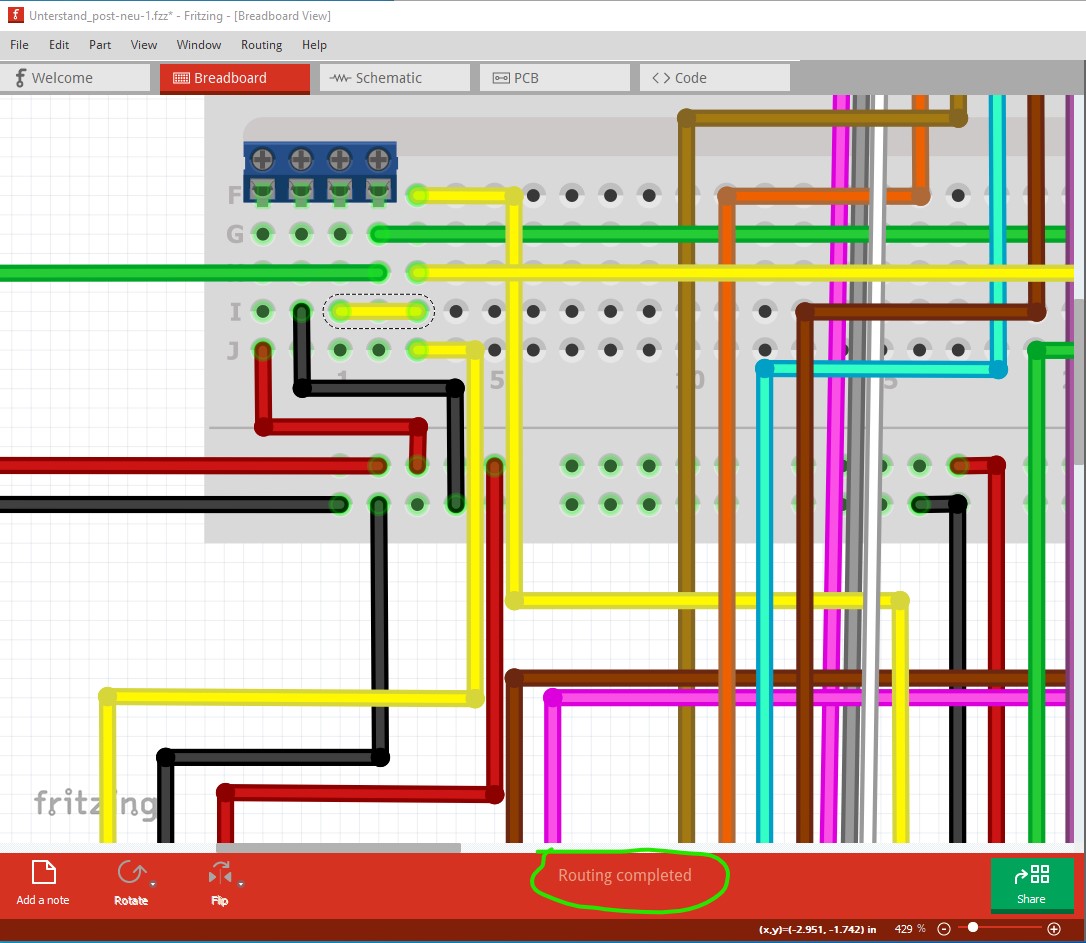
now we should be ready to route pcb. To my surprise Autoreouting and some small amount of DRC movement gives a board that passes DRC. I think a manual routing job would be much better, but this should work …

Unterstand_post-completed.fzz (269.9 KB)

edit4:

Just a reminder I would need the size of the pins on the terminal blocks to verify the holes in the terminal block parts are large enough so the actual part will fit …

Peter

1 Like

Wow, thank you so much for this super detailed reply and all the work you put in the project :open_mouth: :upside_down_face: I really appreciate it.

I will go through everything when I (hopefully) have some spare time this afternoon; just to answer your question about the terminal connectors already:

  • 2 pin connector: distance between pins 0.2 in (5.08mm)
  • 3 pin connector: distance between pins 0.137in (3.5mm)
  • 4 pin connector: distance between pins 0.3in (7.62mm)

Unfortunately, I don’t know what these parts are called, nor do I have datasheets. They were from my parts drawer and don’t have anything printed on them which would allow me to identify them.

These values should be correct. I measured them by hand, then printed my PCB design on paper (1:1 scale) and they fit perfectly when I hold them onto the design.

The only thing I am not sure about the hole diameter (?? my UI is in German, but “Lochdurchmesser” should translate to this) and ring thickness (?? “Ringdicke”). I used a caliper (?? “Schublehre”) and tried to measure them, but due to their very small sizes and my measurement tool not being digital, I could only guess.

That being said, I am considering to purchase those 3 pin connectors with 0.2in (5.08mm) pin distance as well, so they will have the exact same measurements as the 2 pin connectors, but just an extra pin.

the CJMCU2317-MCP23017 part is incorrectly configured

I got this part from somebody’s github. Thank you for correcting it!! Just a general question for my understanding: even though this part is not configured correctly, the measurements and GPIO assignments, indeed, are correct and while DRC failed, in theory I should have been able to use this (incorrect) part as long as the actual/physical parts I used were fine, right?

Either way, I will use your fixed versions from now on for sure. But I am trying to learn as much as possible on the way, so I figured I’d throw this in there.

We would need the data sheet for the relays you intend to use to suggest a suitable driver circuit for the relays (you will likely need to add a relay driver chip to get enough current drive and back EMF protection.)

The relays I am intending to use are these, or at least have the same specifications as them.

Just now I realize that I am missing VCC and GND for them as well. My impression was that I’d need to power the relay(s) it-/themselves via my PCB (5V/GND), but then provide whatever power they are supposed to handle externally (in this case, 12V).

This is all supposed to go inside a junction box. I was going to supply 5V to my board (thus powering the D1 Mini, both MCPs, and all components on the board itself, including the relays); then have two of the relays linked above installed next to the PCB, connected to it, and powered via a separate 12V power source. For this particular project I’d like to control multiple 12V capable water valves.

You would also need to check that the power supply (coming from the WeMos?) can provide that much current.

I was going to use something like this (some 5V power source) connected to the 2 pin connector (labeled 5V VCC GND); this was supposed to provide the energy to all components on the board. Is that wrong?

(lines going through holes)

I can’t believe I missed that - nor that autoroute did it. As I said before, I only had to manually route one single connection. All the other ones were done automatically, and I assumed that fritzing by design would not route anything in a way that would break the circuit… o.O

Again: thank you so much for all your affords effort already. I will look through t he files you provided as soon as I can and report back.

Probably not, as the pcb section of the part is incorrect and did not have pads on the top of the board which would make the pcb incorrect (as well as not routing correctly in Fritzing.

They should work fine without the uln2003 as they have optoisolator drivers and thus should work fine from the MCP23017 pins. If you change to just a relay (without the module), then you need to be concerned about drive current and a snubber diode, but the relay module takes care of that for you.

As long as the pitch is correct, I suspect things will be fine as the parts should standard. The issue is the hole size, if it is too small the pins won’t fit in the hole.

here I have selected on of the terminal blocks, in Inspector (the lower right window) it shows the hole for the pin will be 1.1mm. You need to make sure the diameter of the pin on the terminal block is less than 1.1mm so that it will fit in to the hole that will be drilled. Then check the other terminal blocks the same way to make sure their holes are big enough. The ring thickness is the size of the copper pad and the default should be fine. The important part is that the hole diameter is large enough so that the pin will fit in it.

That is the best way to do it. I wasn’t sure that the WeMos didn’t have a USB connection and was getting the power from there (and USB has current limitations.) An external source of 5V is fine, being external you can easily change it to a higher current model if you need more current.

Normally Fritzing wouldn’t have done this, but because the part is misconfigured and didn’t have pads on the top Fritzing didn’t know that it shouldn’t put traces there, nor recognize that there were holes that were impacting the traces.

Peter

1 Like

Thank you. I modified your Unterstand_post-completed.fzz (269.9 KB) to make the following changes

  • added 2x GND & 5V for the relays
  • connected DMP280 SDA pin (it seemed to have been missing)
  • combined 2 separate terminal connectors for BMP280 (2x2) to one 1x4
  • both relay connectors are now 0.2in (5,08mm), getting rid of the large terminal connector alltogether
  • added / rotated some text

Unterstand_post-neu.fzz (270.0 KB)

About the hole size / hole diameter: as far as I can tell, every single hole on the board needs to be the same size and diameter as the ones used by WeMos D1 Mini and your modified version of MCP23017. When I was prototyping, I used this kind of PCB:

Each and every hole is the same, and each and every component (except for the 3 pin connectors due to pin distance and the large connector I got rid of now) would fit. So they can all fit this size. I believe it is 1.1mm, but I was not able to determine this 100%.

Here is my modified version of your file.

OK, a few problems here. There is a missing wire in breadboard

Indicated by the 36 of 37 nets routed message circled in blue at the bottom. That is caused by the rats nest line (circled in red on the terminal block) having no connection to the breadboard strip with the yellow wires. It won’t currently affect anything because it is correct in schematic and thus the net exists to route in pcb, but it should be connected so breadboard is correct, like this:

Now we get the correct routing complete message at the bottom.

In schematic

the two new wires to the terminal block are not routed and

the new terminal block is neither placed correctly nor routed. So correct both of those:

Then on to pcb where there are problems (and it looks like a bug!) Here I ran a DRC (Routing->Design Rules Check) which checks for traces to close to each other or overlapping each other. It finds a lot of errors!

The area circled in red in the image has a lot of problems, I would guess because of manually moving traces. Some of the traces are overlapping. Rather than try and correct all that (and to make sure the changes I made in breadboard and schematic really were correctly reflected in to pcb!) I chose to do “Routing->Select all traces” then hit the delete key to delete all the traces in pcb. Then I selected “Routing->Select all vias” and hit the delete key. This deletes all the traces and all the vias that autorouter added. leaving me with this:

just the parts and rats nest lines with no traces or vias. Now I ran the autorouter and then ran DRC again. There are still issues (which is likely a Fritzing bug as autorouter should not be producing DRC errors while routing!) In this image I clicked on the first error in the DRC list which then highlights the wire that it is complaining about (circled in red)

the red line on the top of the pad indicates where the trace that is too close is (in this case on the bottom layer which is covered by the trace on the top layer!) So at this point I selected View and disabled the copper top layer by clicking on its entry to unselect it.

which produces this:

which shows only the bottom layer traces (making the red marks easier to see and correct!) The trace circled in red has red marks on all the pins of the MCP23017 part so moving it up slightly to increase clearance clears the problem. Doing the same thing for all the rest of the errors creates this sketch which now passes DRC successfully

which was created from this sketch.

Unterstand_post-neu-fixed.fzz (273.3 KB)

I will report the autorouter DRC issues on github as a bug after experimenting with the grid size as this may be a case that the grid size is set too small.

Peter

I don’t think that autorouting uses the grid size / align setting. At least I remember bend points ‘snapping’ when moved after autorouting was done.

A possible fudge for the DRC problem, is to increase the keepout distance setting a little before doing autorouting, then decreasing it again before doing design rules check.

Routing ¦ Autorouter/DRC settings… ¦ custom ¦ Keepout

I figured I could do that, but I shouldn’t have to. I opened an issue on this on github because it is desirable that autorouter by default generates a route that passes DRC and it appears at present the defaults are set incorrectly.

edit: and indeed when I set the keepout from 0.01in to 0.025in ran autorouter and then set keepout back to 0.01in and ran DRC, DRC passes. Autoroute took longer to complete, but it did route without having to increase the iterations.

Peter

Sure. Just providing a possible work around until the real problem gets fixed. And from your test, that worked.

Thanks everybody.

The PCBs are on their way. I will report back once I tested the boards. Really excited for this project :slight_smile:

I actually ordered an earlier version of the gerber file than the final one. I don’t believe it, but I really did. So there are multiple things I had to manually solder in order to make it work.

I will start from scratch by using MCP23017 microcontrollers (?) rather than those dev boards I had used here. Also, I didn’t realize that while the D1 Mini can handle 5V, it can only be powered via 3V3. This would be fine (I can power the D1 and the mcp23017s, and most sensors via the D1 USB port), but the PIR sensors I added need 5V (or at least they don’t work at the moment powered with 3V).

Should I open a new thread for my new PCB or continue here? Also, what would you recommend to use for the main power? I currently thought I’d use a 5V power source that everything could run on. However, unless I use different PIR sensors, I’d need both 5V and 3V3 for this project.

Can I use resistors? For example, perhaps even use a 12V power source (so I could power the relay board as well), then but resistors between this power source and tune it down to 5V and 3V3? I do have buck down converters, however, those are external components again, so if resistors could get the job done as well (which I could also integrate in the new PCB), I would prefer doing so.

continuing here should be fine.

The main deciding factor is what is the power source? For batteries, you want maximum efficiency for battery life, if you are powering off the power line, efficiency is less important. A 12V source (to drive the relays) with a buck converter module (for efficient transformation of 12V to 5V) and a LDO (low drop out) linear regulator for 3.3V would do the job best probably. A more efficient but physically larger option would be another buck converter module (which can be physically quite small!) to provide 3.3V from the 12V supply. Resistors are a bad idea, both because of efficiency and because the voltage changes with current (the buck converter is regulated, a change in current will not cause a change in output voltage!)

Peter

I thought of using something in the likes of a INPUT: 100-240V ~50/60Hz 2.0A / OUTPUT 12V 2000mA (or similar, this is the one I currently have) plug. I also own a bunch of these (links to some random shop, no affiliation) LM2596 DC DC Buck Converters.

They can take 4-35V input and will output between 1.23V - 30V. I would need two of these, one to turn my 12V input to 3V output for the Wemos D1 Mini (which I might replace with a generic esp8266 chip to save room) and 5V output for whatever sensor/actor might require it (for example, the PIR sensors I still have a bunch of and planned to use; I also ordered a few AM312 PIR sensors, which run in 3V, but the mcp23017 can run on both 3V3 and 5V, and I thought it’d be better to have both available because the device I am building is supposed to be used for different projects with different components.

So I’d have three different voltages through the board, the original 12V (as input to be connected to the converters as well as output to power the relay board), the 5V (for the old PIR sensors or “just in case” if I use the other PIRs), and 3V3 for the ESP board and everything that needs it.

Just an idea: as in the old layout, I had a couple of “free” pins that could be utilized in other projects. These could easily have a 3V/5V jumper so that they could manually be set for whatever voltage the component might need.

The LM2596 should be fine for this, right? However, you mentioned smaller components, perhaps some that might be easier to integrate when designing a new board? These ones here need to be screwed to the board (they have two I believe 2.5mm screw holes), then connected somehow, they expose for holed metal plates on the corners, 2xIN, 2xOUT).

Yep the Mini-360 DC-DC Buck converter (available from amazon, ebay, etc) is a lot smaller and there is a Fritizng part (Mini-360 DC-DC Buck converter.fzpz) for it posted here in the forums. It looks like this compared to a LM2596:

so is much smaller. 1.8A output continuous which should be lots.

Peter