This is what I mean with plated-through slots.
I recently managed to desing a pcb with plated-through slots to solder a Li-ion 18650 battery with soldered nikel U-tags.
To achieve such thing I had to design 2 things:
1st → A custom pcb svg with pads
2nd → li-ion part footprint with platted slots
Then I had to make both things match in the pcb layout. If I wanted to move the li-ion battery position in the layout, I had to redesign the custom pcb svg. It was a pain in the a@#.
Before reaching this point, I ried to modify li-ion footprint svg with “<path…” instead of “<circle…” in cooper layers, but fritzing wont generate the correct gerber file. I guess fritzing only understands drills when you use circles in cooper layers.
I also tried several drills together, but it is a horrible work-arround and most PCB manufacturers wont accept that solution as it can break the drill.
Don’t do this please:
So the question is:
¿Is there a way to desing a part that produces those plated-through slots in the gerber?
This is a feature we hope to implement. See also Cutout part · Issue #3320 · fritzing/fritzing-app · GitHub (and probably others).
Did you try changing the orientation of the path? Like instead of clockwise, route the outline of the cutout path counter clockwise. I tried but it seems that is not the trick.
There are group ids (layers) like “board” and “boardoutline” used in Fritzing parts, but I could not create a part that would cut from a board. The board group is not rendered in Fritzing, and neither does it apear in the gerber contour file.
I think there are two approaches to improve Fritzing here
A) add support for a generic “boardoutline” layer in parts, that can be used to add or cut boards.
B) add support for rectangular cutouts.
So i guess my approach is correct up to date.
Just in case this is helpful to somebo:dy
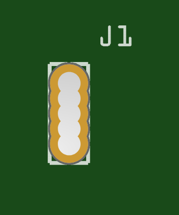
I managed to get a correct gerber file adding all needed cutouts inside boardoutline layer. See this svg file: (rename extension to “.zip” as i can not upload zip to the forum)
custom.fzz (519 Bytes)
No matter if it is clock or counter-clock
You just need to define the paths you want the milling machine to follow. No need to do substractions in svg editor or something like that.
You should also define the milling tool width, using the “stroke-width” in the svg but fritzing does a mess with that in contour gerber file, so i dont define any width.
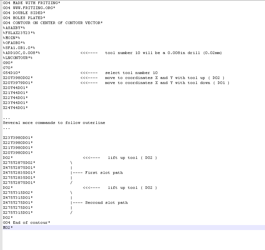
This is the gerber result i got: (excuse my gerber translation as i’m not an expert)
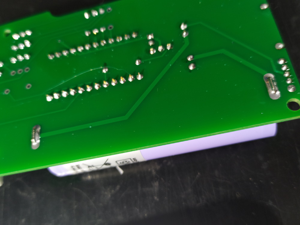
And as you can see in the previous photos i got my pcbs as intended.
WARNING: I talked to produccion people before ordering the PCBs and they advised me to add a comment in the order: “Slot in GM1 need to be milled” just for they to check machine was correctly translating the gerber.
1 Like
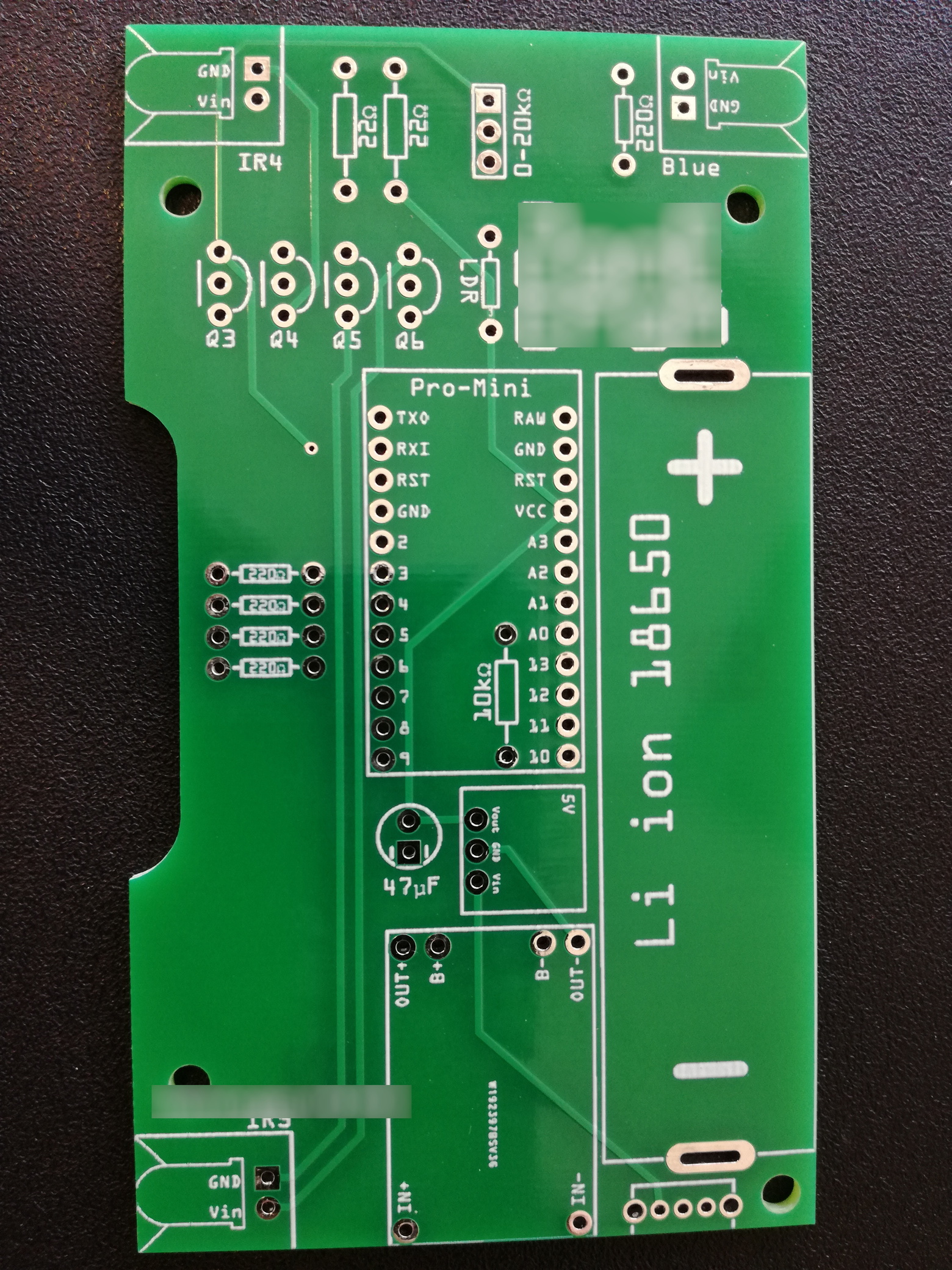
Just for reference, that gerber code has produced this PCB.
Note that the slot is defined in the custom PCB svg and the plated arround slot is defined in the part SVG, so you must be careful aligning them.
I have blurred my commercial logos.
1 Like