Hello everyone, I have made an updated version of my PCB, it will be a Work In Progress for a bit so any in put would be grate. I’m new to making PCB’s and electronics so if you see any errors with either the layout or circuitry please let me know. I am also happy to answer any questions you may have about the PCB or my Project. I have also completed the Arduino code if there any coders who want to see it, but it is not neat by a long shot as i am new to coding as well, there are plenty of notations though.
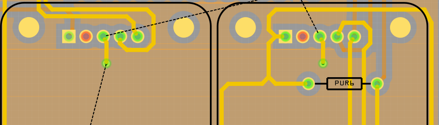
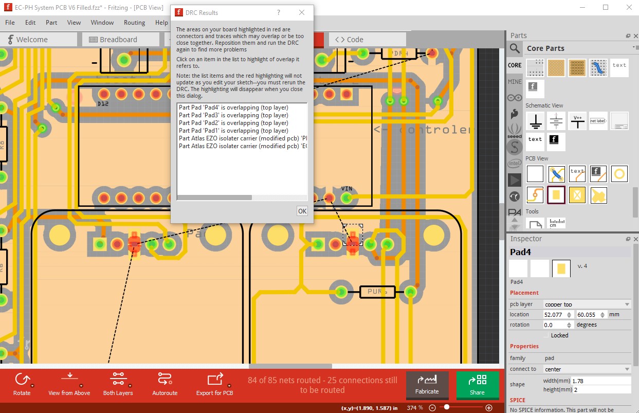
Also I am having an issue with the ground fill not connecting to the Atlas scientific Carrier PCB. I checked with Peter who made it and the part is made properly, so I did the ground fill then I ran a trace on the top layer to a via I place after completing ground fill so it connects. is this going to make a popper connection when i send the PCB to be printed?
Image 1:
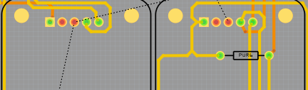
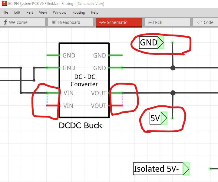
Image 2:
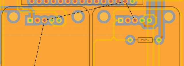
Image 2:
Finished file with copper ground (bottom layer):
EC-PH System PCB V6 Filled.fzz (304.0 KB)
Finished file without copper fill:
EC-PH System PCB V6 UnFilled.fzz (213.5 KB)
Thank you,
Tyler
A couple of issues (all minor!): schematic has two unrouted nets
vin and vout are connected together in pcb and thus reflected as rats nest lines in schematic (and caused a routing not complete message.) As well the connect bug is showing up on various of the net labels. Moving them slightly appears to fix that so I did that. In pcb the ground fill appears to have worked fine, but there is a better alternative.
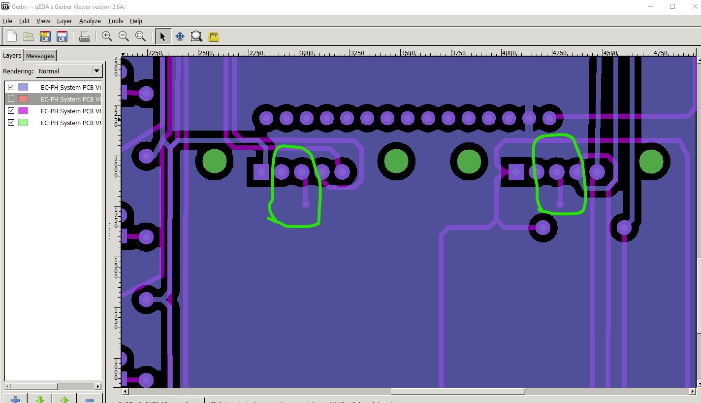
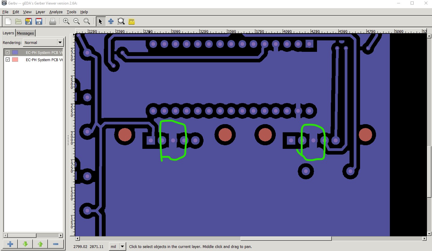
This is the gerber output from the sketch, as we see there is copper to the ground on the carrier boards as desired. However there is a better way to do it that avoids the vias:
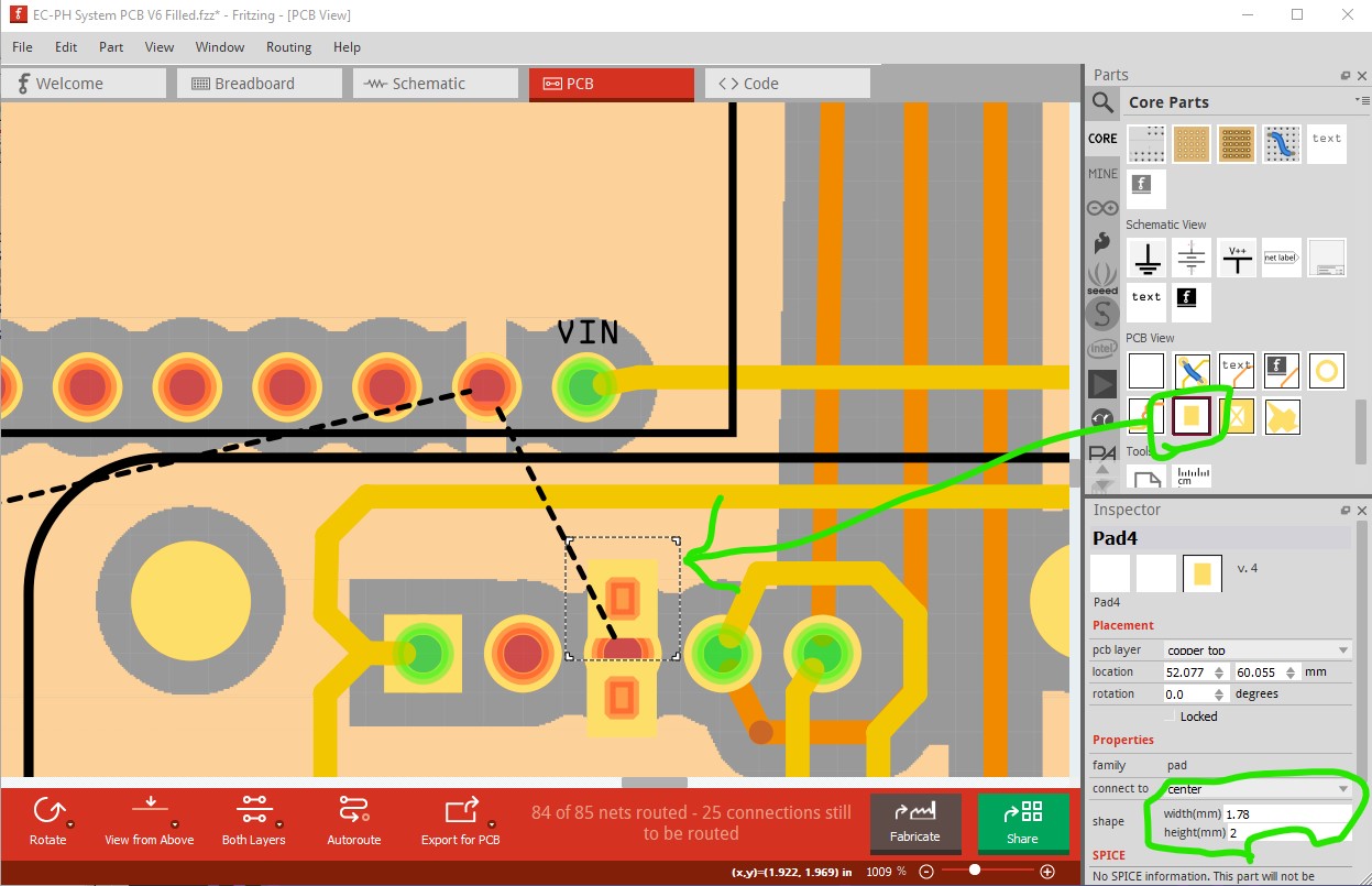
drag a pad in from the pcb section of core parts and change its size in Inspector to be the same size as the pad and move it to the bottom layer. Then overlay the pads to create the same connections that copper fill should have (I disabled View->align to grid to let me move it to the center of the pads!). This causes a DRC error because the pads overlap with the carrier part, but we can ignore that.
on the gerber output it does the right thing, connects the grounds as copper fill should have (the copper fill bug is being worked on but isn’t fixed yet!)
These changes are in this sketch
EC-PH System PCB V6.1 Filled.fzz (304.6 KB)
Peter
Ok thank You, This is very nice, just out of curiosity are vias best to avoid? if so is it because of any specific reason?
Thanks,
Tyler
Vias are a potential point of failure (as the plating through can fail) so using as few of them as possible is a good practice. Sometimes they are unavoidable (such as when traces need to cross over one another) though.
Peter
OH, alright that is good to know
Thank You,
Tyler