Properly manufactured vias from a PCB manufacturer have copper plated holes so don’t need solder in them, but you can solder them if you want.
Your SCH view has junctions in the wrong places and the 3.3V and 5V are on top of traces.
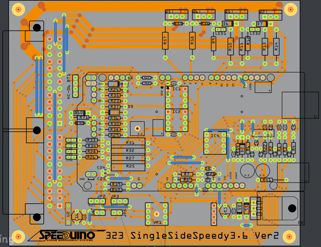
Not that it matters in such a simple circuit, but in PCB new designs use 45º corners instead of 90º. For neatness use the grid snap and make distance between traces more equal.
Something like this
Watch part 2 and 3
Check your design before getting it manufactured or it will come back wrong. Watch part 3
Look up the datasheet for that 3.3V regulator and look for a recommended/application circuit, because regs usually have caps on the pins.