So, after 101 checks of my board design, I sent it off for a set from a popular house in Asia. The boards came back looking very nice, but ended-up being $70 of trash. The issue is that everything measured correctly in Fritzing, but the board hole spacing does not match that. So, I’m asking if the error might be on the factory side, or if it may be on the Fritzing side, as I can’t do many of these mistakes. I might also get some credit if it was the board house causing the error.
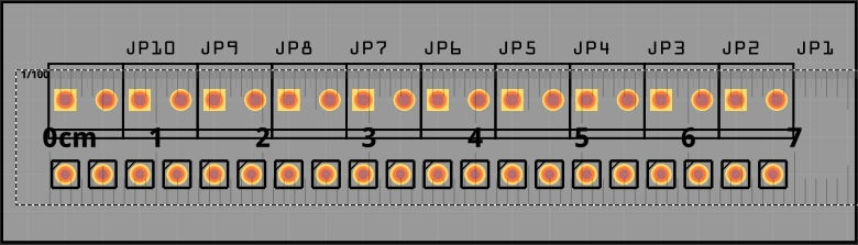
Here is how to duplicate: I used a string of ten (10) 3.5mm 2P screw terminals from the Core parts. I made 10 and spaced them with 3.5mm grid spacing. In Fritzing, the part holes are wrong (should be 3.5mm, duh), but holes measured less than 0.5mm off, and the actual OAL of terminal blocks came-out right-on at 70mm using the Fritzing ruler.
When the board were made, the holes were 68.6mm center-to-enter at the ends (not 66.9 with part error) and the overall of the silkscreen part outlines were 72mm (not 70mm as Fritzing measured). This is just big enough to make for very poor assembly at best, and are really not acceptable. Can anyone shed light as to why the actual PCB does not match the Fritzing dimensions? Can I prove the error was theirs, or am I stuck with junk boards? Any insight welcome!
Can you post the .fzz file of the sketch? As well you should check the gerber output (file->export->for production->extended gerber) with a gerber viewer (I use gerbv) to see what the board house will make. That is essentially what I will do if you post the .fzz file to tell you where the problem is.
Are these the plain lockable 2pin screw terminals or the plug-in type with a male and female, because the latter doesn’t have 1 continuous pitch when resting against each other - the 5.08 does but smaller doesn’t -.
Thanks, Peter. I have Gerbv, and will attempt to make better measurements with it. In a round-about way, you answered my primary concern that this has happened to others or not, by not saying so. I searched but could not find a similar issue.
For the holes the drill.txt file is your likely easiest answer. The format is plain text with the hole size in the first set and the x/y coords in thousands of an inch in the list of holes (grouped by hole size) under it. It is somewhat unlikely (but not impossible) that the board house did it wrong. It somewhat more likely that Fritzing did something wrong as even some of the parts in core are not correct. As I said if you upload the fzz file one of us can probably tell you where the problem lies just by looking at it.
Thanks, but that file is not at my location, and I just made that image above to represent. Id’ rather upload the actual file, as that’s the one that counts.
Yep. But that is a lesser issue, compared to the 2.8% larger spacing actually made, it becomes unusable. The pin spacing issue is not multiplied through the number of blocks. Only in each block, as imaged above. But grow it, and If nobody has had an issue with long strings of holes like this, then it has to be a board house issue, and I just need to find it.
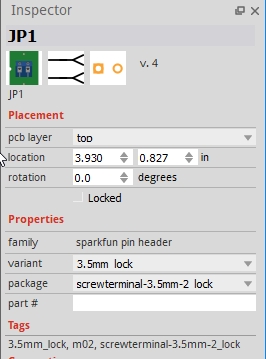
The pcb svg shows the pin spacing to be 3.855mm and that the part was generated by the eagle to Fritzing library. The Sparkfun site doesn’t have a data sheet per se but they do claim the spacing is 3.5mm (which this part is not …) so there is a good chance the part is wrong is the problem not the board house.
I’ve got a theory. The production house might have seen the 3.81mm terminals and spaced them all at 3.81mm. If you subtract 3.5 from 3.81 you get 0.31mm, and if you times that by 9 it’s 2.8mm, closer to 72mm than 70mm. Measure the holes with a vernier and see if they go 3.5mm, 3.81mm, 3.5mm etc, or 3.81mm etc.
If it was me I would just sand off the locking tabs and use the PCBs.
OK, so I did some tight measuring in GerbV as suggested to me, and indeed the gerber’s row of blocks is 70mm on the nose. So, I measured the PCB with calipers and it is also about 2.6mm oversize. It would seem the whole thing “grew” a couple percent, but not in the Firtzing output. it seems (other than the incorrect 3rd party part pin spacing) that Fritzing did its job. Thanks for all your help and suggestions!
PS: Old_Grey, the board is oversized a bit, so the block tabs are not the issue, and in-fact they are not working like they should. So, it looks more like a social party than a row of soldiers.
There is something wrong with that because nothing would ever fit if every time you sent it for production and it was scaled up. A 40pin straight-line header would have trouble fitting with a 1% scale, yet alone a 3%. I would be checking the dimension of 2 far apart holes perpendicular to the screw terminal row on the PCB and comparing it to what it’s supposed to be in FZ - the size of the PCB compared to FZ size might be enough -.
If you could post the drill files or the exported files (Gerbers). I can also check them out as I work for a proto-type board house in the USA.
Old_Gray mentioned a theory about the production house making changes based on the parts. I have never seen a board house care about what the part is and Gerber data has no information about the parts. So I do not see them fixing spacing issues as they don’t have time or know what you really wanted…
There is also the possibility that you hinted about, the board house scaled up the data. This could happen as they have to account for the manufacturing processes. If the job was treated as a multilayer or was on very thin material it would have to be scaled up.
(Scale factors are based on the Material type, thickness, copper weight, layer types (signal, plane, mixed) and mfg panel sizes. ) The goal is to get a correct finished size board in the end but mistakes do happen.
 If nobody has had an issue with long strings of holes like this, then it has to be a board house issue, and I just need to find it.