I’m completely new to electronics and PCB. I designed a PCB for my railway hobby that came back from manufacture with a short between ground and +ve. Clicking on any of the connectors highlights the other connectors in yellow but no obvious short. Any help on what I screwed up would be greatly appreciated. Many thanks.
A quick (very quick) look suggests the copper-fill is touching some Pads (and trace).
I recommend a complete review of your board.
You can start by saving a copy and delete the copper-fills to reveal Pad & Traces issues.
Sure, you can turn off the fill layers but won’t be as clean as deleting it. After/If not finding issue witl PAD/Traces, add the fill back and check it out…
Work on one layer at a time…
Image of fill touching (perhaps intended but, perhaps Not…)
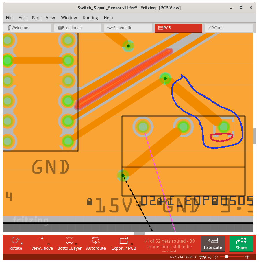
As far as I can tell, there are no shorts between ground and +ve in the Fritzing sketch MODEL (the nets). However, I think the problem is in the copper fill (ground fill). Here is a snapshot from a section of your pcb showing only the bottom layer. Notice that the 3rd pin, which is VE, is connected to copper fill, but so is the 2nd pin, which is gnd.
Here is a snapshot of the same area, after I removed all copper fill, explicitly set the ground seed to be (only) pin 2 of the part, and did copper fill bottom. Notice that there is now a keep out area around the trace highlighted before, and the pin 3 connector is not connected to the copper fill anymore.
I suspect you managed to set a bad group of ground fill seeds before doing the ground fill. At least on the bottom. I did not check the top, after spotting this on the bottom.
Fritzing really should have reported this, either as part of the Design Rules Check, or when setting the ground fill seeds.
This is something that should have been fairly easy to spot, by using a Gerber viewer on the export before sending it off to be manufactured.
EDIT: Late thought. Did you perhaps add more traces after doing the ground fill? Fill should be the last step. If you need to make changes, remove the fill, do the changes, reapply the fill.
Not really. Connector and traces, though you should not need to measure the keepout. Just make sure it exists. There are multiple bugs reported against the Gerber export code in Fritzing. You really need to look at what was generated (in a gerber viewer), and verify that it did what you expect. Most of the potential problems are more obvious, like a drill hole in the wrong position, or totally missing. Sections of silkscreen that are missing. This one can be seen directly in the Fritzing PCB view, once you know what to look for. Any ‘trace’ that is ‘on top of’ the fill area on the same side is actually connected. It is all copper, all on the same side, with no insulation between them. Setting the view to show only one side at a time makes it more obvious, easier to check.
As @microMerlin said there isn’t an easy way. The best practice is to do the gerber export, then us a gerber viewer outside of Fritzging (I use gerbv from the Geda project but there are lots of gerber viewers) to check the various layers for errors as the gerbers are what will produce the board and that occurs after all the rendering in Fritzing (and as noted has bugs of various kinds.)