I ran the rules check in Routing and got some errors that I need help interpreting:
According to the first one for example, “2 pins on J7 are overlapping” and so on for all others. Why are they overlapping? Take J7 for example which is the top-right 2-pin header I used for the tiny. One pin goes out the top layer and the bottom pin goes out to top and bottom but in different directions, so they shouldnt overlap.
What am I missing?
It looks like you have the hole diameter of the header pins set to a very large size. So large that it causes the rings to over lap each other. Select one of them and then in the inspector change the size of the holes and rings.
Here is the inspector. Those options are greyed out so I cant modify them 
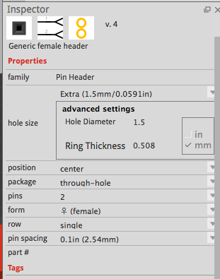
I don’t see anything greyed out. I do see you have it set to Extra 1.5mm which is the cause.
It will only be greyed out if you have clicked on one in the bin. You need to click on one on the board and then you can change its settings.
Glad to help.
Your problem is most likely a result of scrolling while in the inspector. It has the nasty effect of changing values and you don’t always notice when you do it.
