It took me a bit of time to work out a process that works well enough, and consistently enough for my needs. I used various posted tips and the (old) how-to-do-it documentation and I’m posting this simplified approach…
This works with Inkscape and EZDraw. It will probably work with other drawing software as long as it has ‘Layers’ to draw on with re-namable ID’s.
SVG files are XML Text files and can be opened/edited in text edit software and re-naming can be done this way, too.
Various versions of the drawing app’s I used seem to change with their revisions (especially OpenSource) so, to the point, the need is to edit the XML file and change the ID of the layers. It’s as simple as that. Inkscape does have an embedded XML editor with a display panel.
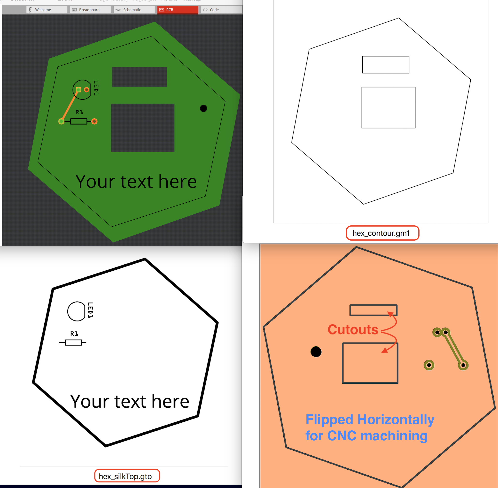
It doesn’t matter what’s called a hole or cutout… they need to be Boolean Difference’d from the PCB board (but, done on the same board layer). Silkscreen is on a separate layer.
Inkscape will need to generate Object to Path, whereas EZDraw takes care of that automatically.
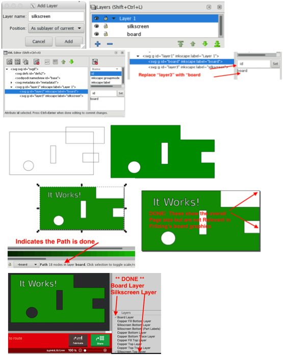
Screenshot attached showing various steps described below…
HERE WE GO:
Inkscape
1) Create two sublayer’s for the default ‘Layer 1’ and place them in this order
⁃ Layer 1
⁃ board
⁃ silkscreen
2) Open the XML editor
⁃ Edit > XML Editor
3) Select the top line of the “Silkscreen” group
⁃ Note: the “Label” is not important, the “ID” is important
⁃ Select ID, and enter “silkscreen” and press Set button
⁃ simply replace the defaulted text (
4) Repeat #3 for the “board” group
5) Select the ‘board sublayer’ and draw the PCB perimeter shape (such as Rectangle)
⁃ Select the PCB perimeter
⁃ Select from Menubar: Path > Object To Path
⁃ WAIT!!! It may take 15 seconds to process. Look at the bottom of the screen for indications that it finished before going further
⁃ Draw the Holes, Cutouts… other
⁃ Select the PCB perimeter and only ONE of the Holes, Cutouts, other
⁃ Select from Menubar: Path > Difference
⁃ WAIT!!! It may take 15 seconds to process. Look at the bottom of the screen for indications that it finished before going further
⁃ The Hole (whatever you used) will now be incorporated into the PCB perimeter/shape.
⁃ Repeat for each of the Holes, Cutout…etc, doing one item along with the PCB shape at a time until all except for the Text or other graphic for silkscreen are done.
⁃ If desired, select the PCB shape and Fill with a color
6) Switch to the ‘silkscreen sublayer’ and draw items, such as Text
⁃ Recommend (as a starting point for Text) use:
⁃ Stroke = 0.25mm
⁃ Fill = none
⁃ Stroke paint/color = white
⁃ Stroke Style Width = 1mm
⁃ Select the PCB shape and the Text
⁃ Select from Menubar: Path > Object To Path
⁃ WAIT!! until done
7) Save As Plain SVG
That’s it, now can use it in Fritzing
EZDraw
1) Create two layers: board and silkscreen
2) Draw PCB shape and Holes, Cutouts on the ‘board layer’
⁃ Select PCB shape and One Hole
⁃ Select from Menubar: Tools > Combine > DIfference
⁃ Repeat for each item
⁃ Fill with color if desired
3) Draw Text/other on the ‘silkscreen layer’
4) Save as SVG (1.1)
5) Open the SVG in a Text Editor
⁃ Look for the ‘board’ and ‘silkscreen’ layer groups
⁃ Edit the ID to ‘board’ and ‘silkscreen’ (they will probably default to include something like “layer_board”. Simply delete the “layer_”
6) Save the file
That’s it, now can use it in Fritzing
UPDATE:
FreeCad
The Draft workbench can be used to draw PCB that opens correctly in Inkscape. (In Draft wb, open Preferences, and set the Import/Export>SVG to Raw for CAM.
Now, simply draw the PCB in Draft, Export the full list of drawn items, and Export the SVG. Then, it can be opened in Inkscape. You can simply Bucket fill with color (no need for Path Differencing) or, create the layers as noted above…