hi there, I created a round pcb in fritzing using inkscape to make a svg. in fritzing it looks perfect just as i want it, but when i upload the gerber export folder to pcb company their preview shows the file as rectangle pcb with my custom round pcb inside the rectangle. Now I am worried to order the pcb from the company in case it arrives as their standard preview rectangle shape which i cannot use. What to do please?
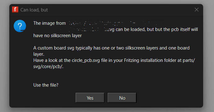
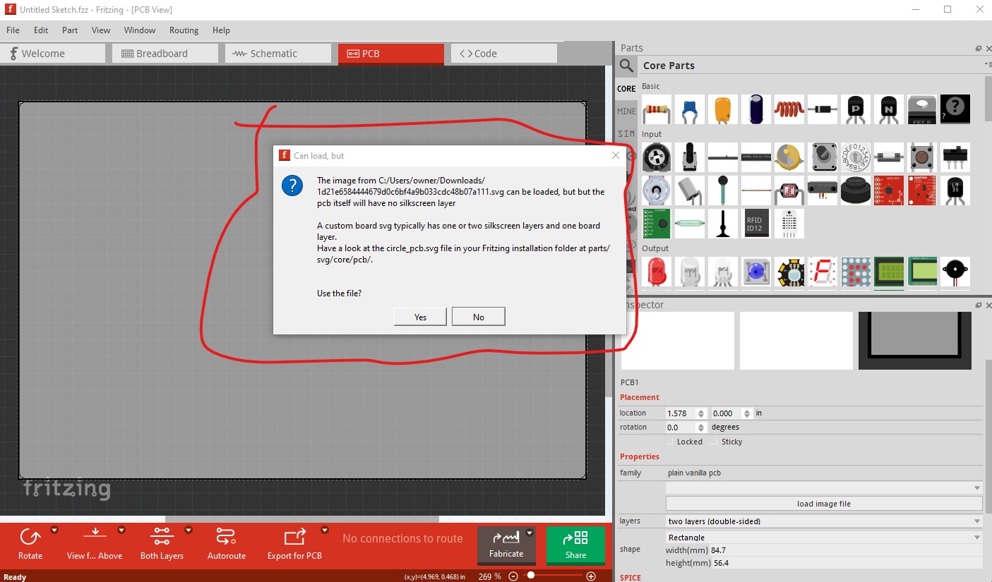
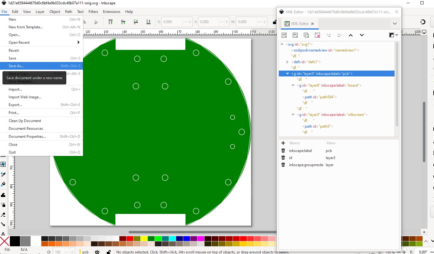
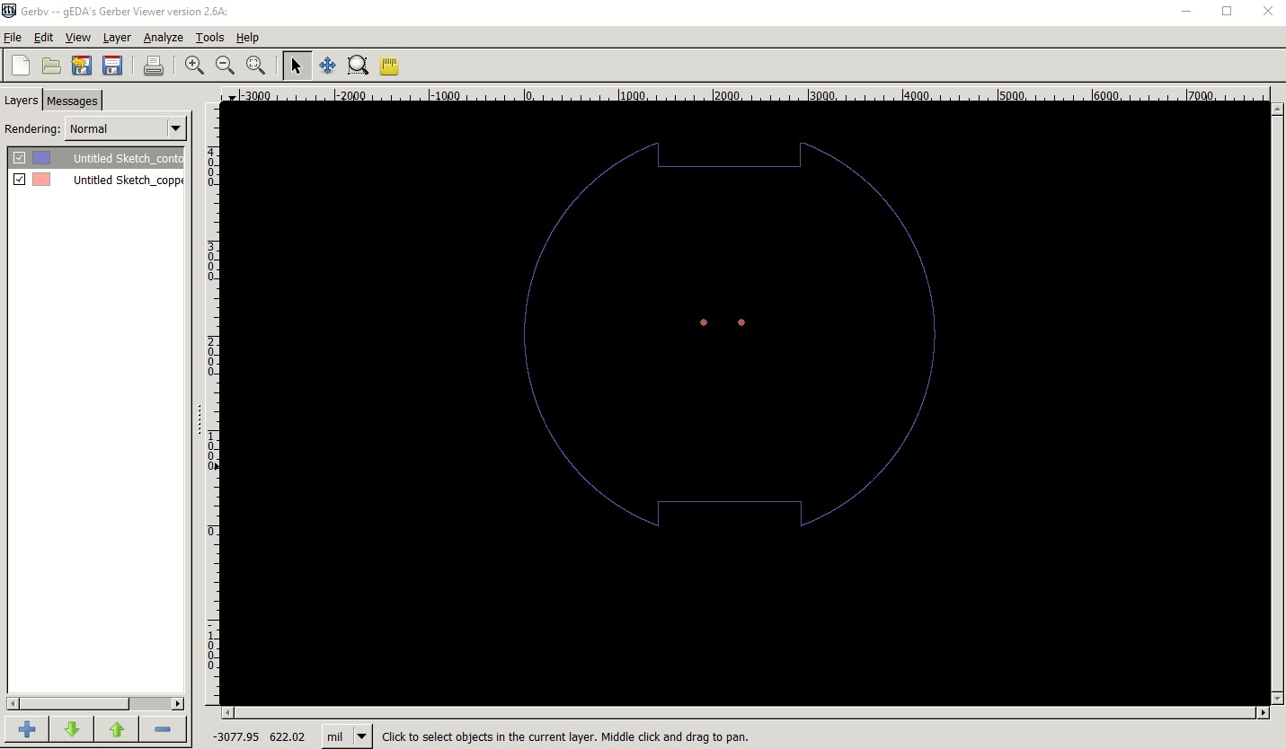
Up load the sketch for your board (the .fzz file, upload is 7th icon from the left in the reply menu.) Then I can create gerbers from the sketch and display them using gerbv (as can you) to verify them. Did you load your custom shape in the the sketch and get no error messages? ? Is the format of the outline svg correct? with both a board and silkscreen group? This looks like you have only silkscreen in the outline svg and it is missing (or misconfigured) and not loading the custom shape (although it is impossible to tell from pictures, always upload the sketch!)
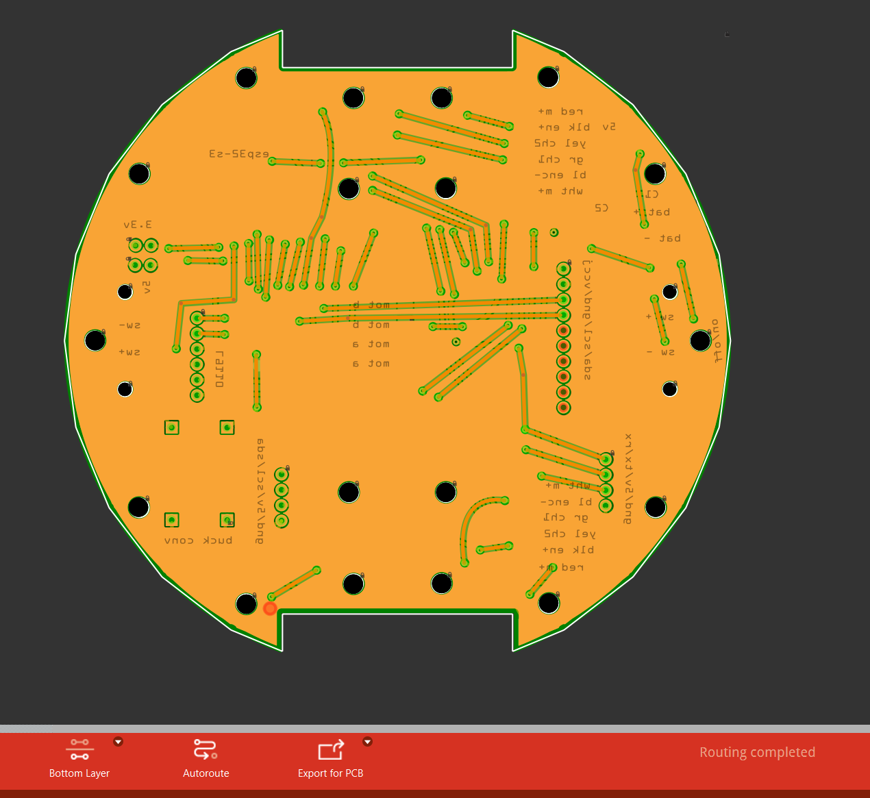
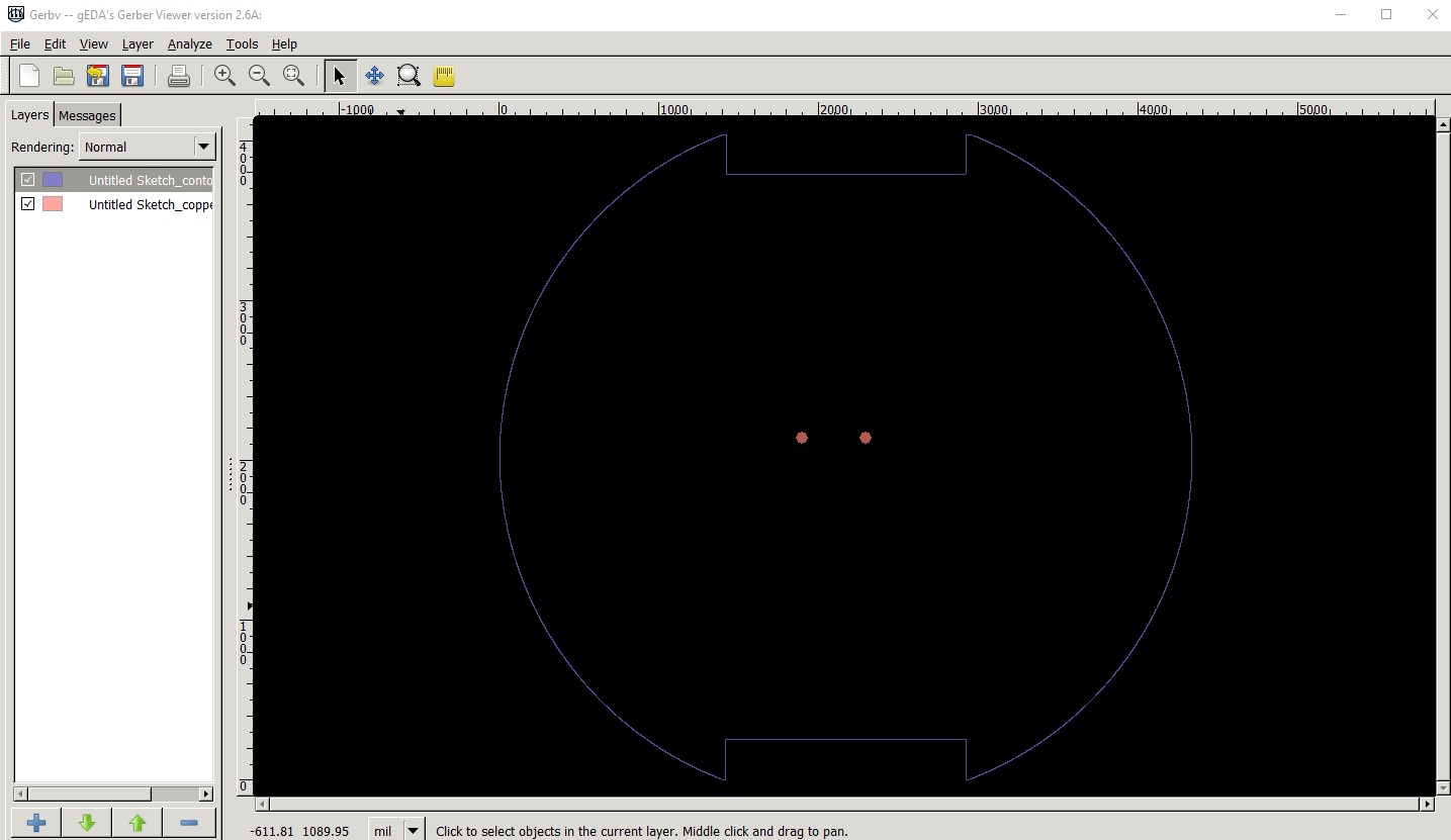
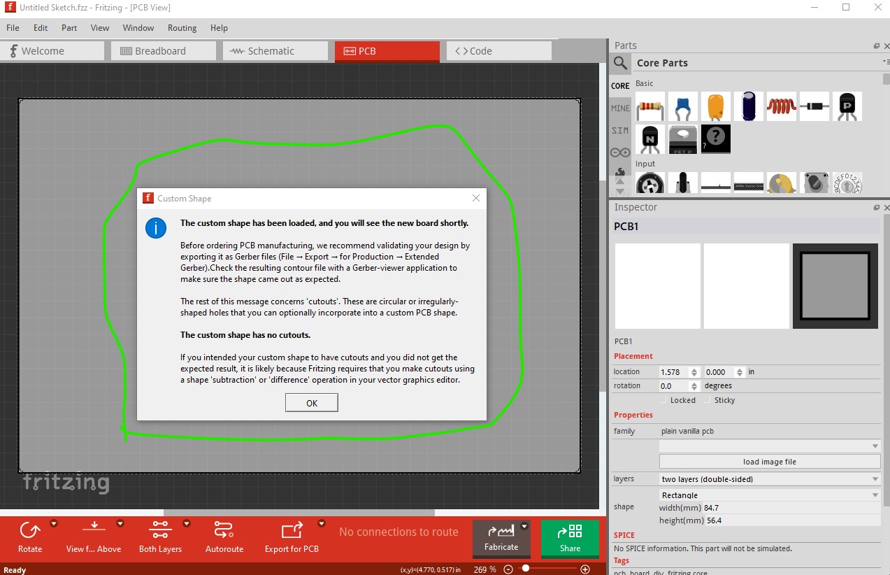
It has the correct outline so in theory should mill the board correctly.
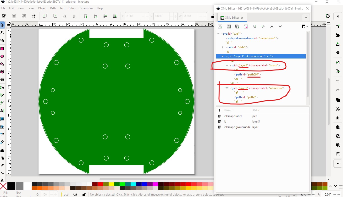
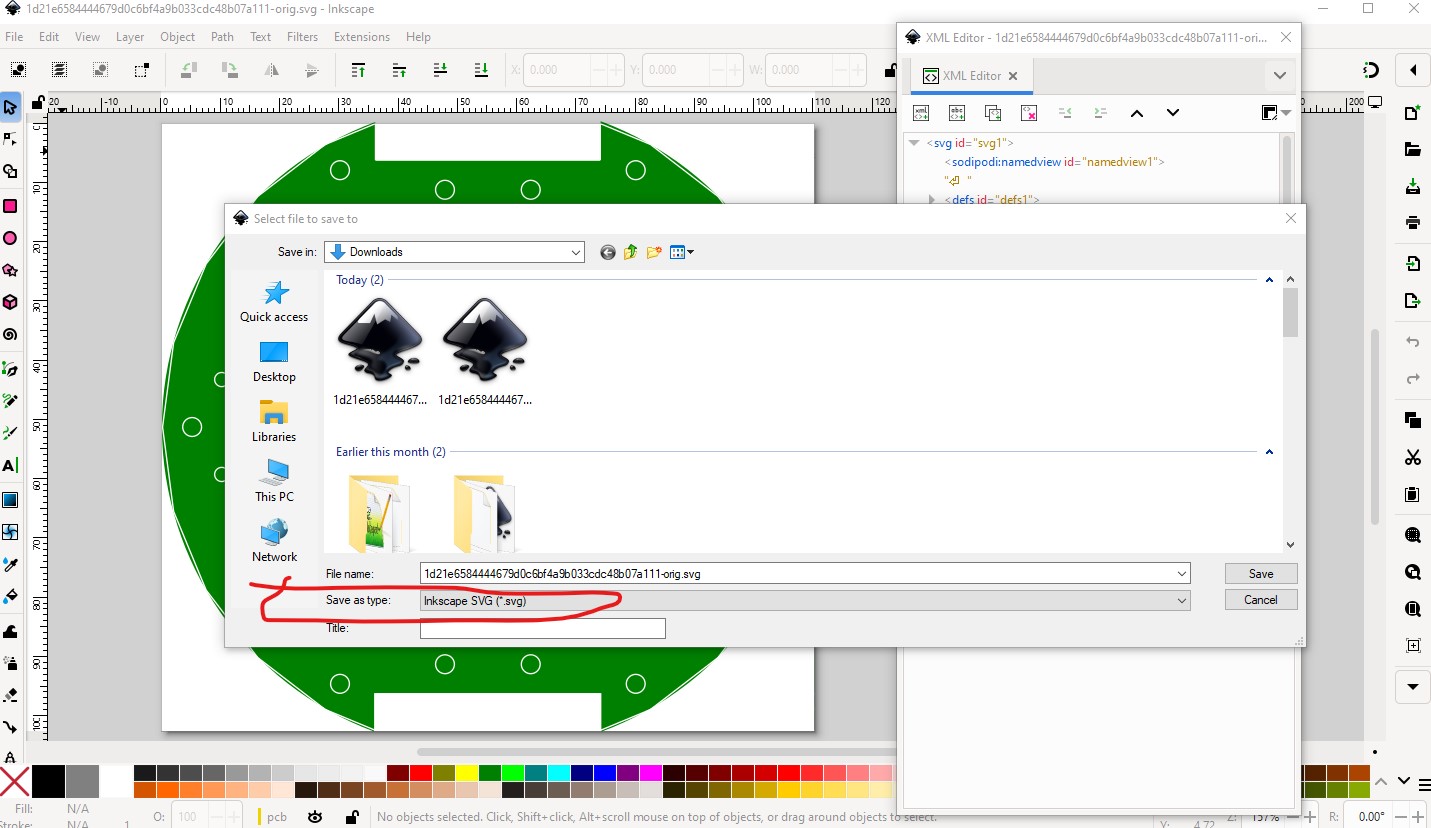
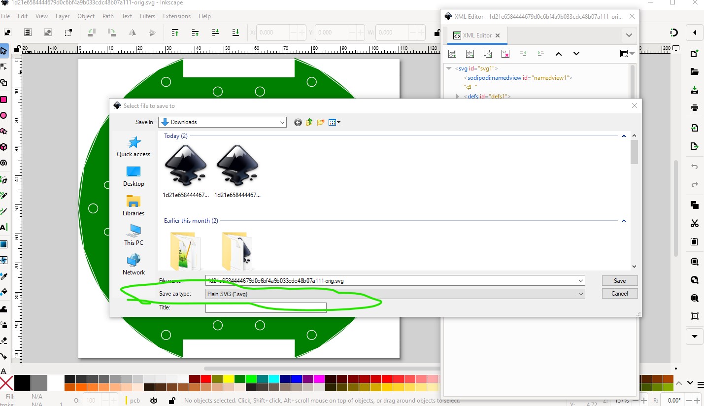
Your svg looks like this (which is incorrect.) The svg id needs to be board (not the Inkscape label!) and the path needs to be id boardoutline. It is best to ungroup the svg and then redo the groups with the correct names then save the svg as plain svg rather than Inkscape svg,
then change the type from Inkscape.svg which is the default (and adds all kinds of Inkscapeisms to the svg some of which Fritzing objects to.) You should do this for all svgs intended for Fritizng. I prefer to ungroup the entire svg to remove all transforms (in the past Fritzing has had problems with transforms) but current versions are improving but it is still worth doing to avoid problems.
It doesn’t complain about the format of the svg this time. It doesn’t appear to make any particular difference though, the contour.gm1 file in gerbv looks identical
Try this svg (to download it, right click on it and select “save image as”
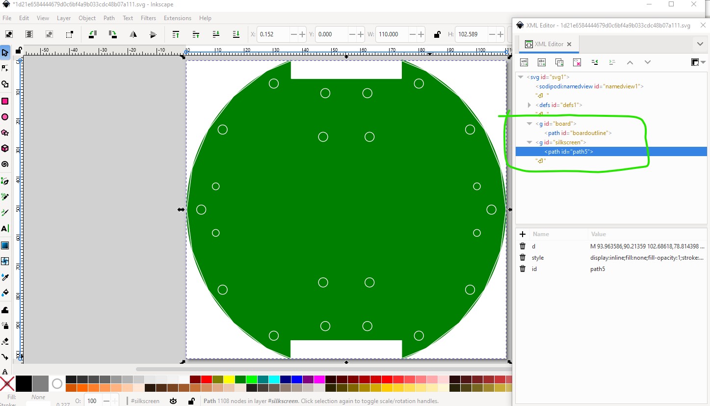
In Inkscape it should look identical to to my image above.
Note none of the hole in the silkscreen will be drilled, I am assuming they are just for alignment purposes and you are dragging holes in to your sketch if you actually want holes there. They can be milled in the outline.svg file but it is a lot more complex. Try the new svg and send the gerber output to your board house again and see if there viewer looks happier. I would say the either contour.gm1 file should correctly cut the board outline, but I’m not dead sure of that. The lack of the correct labels may have broken gerber processing in Fritzing although the contour.gm1 file looks OK to me it may not really be.
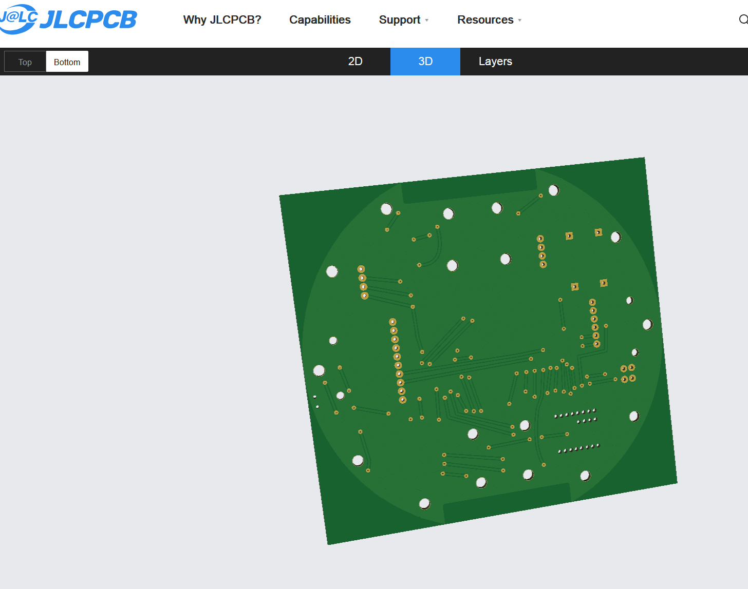
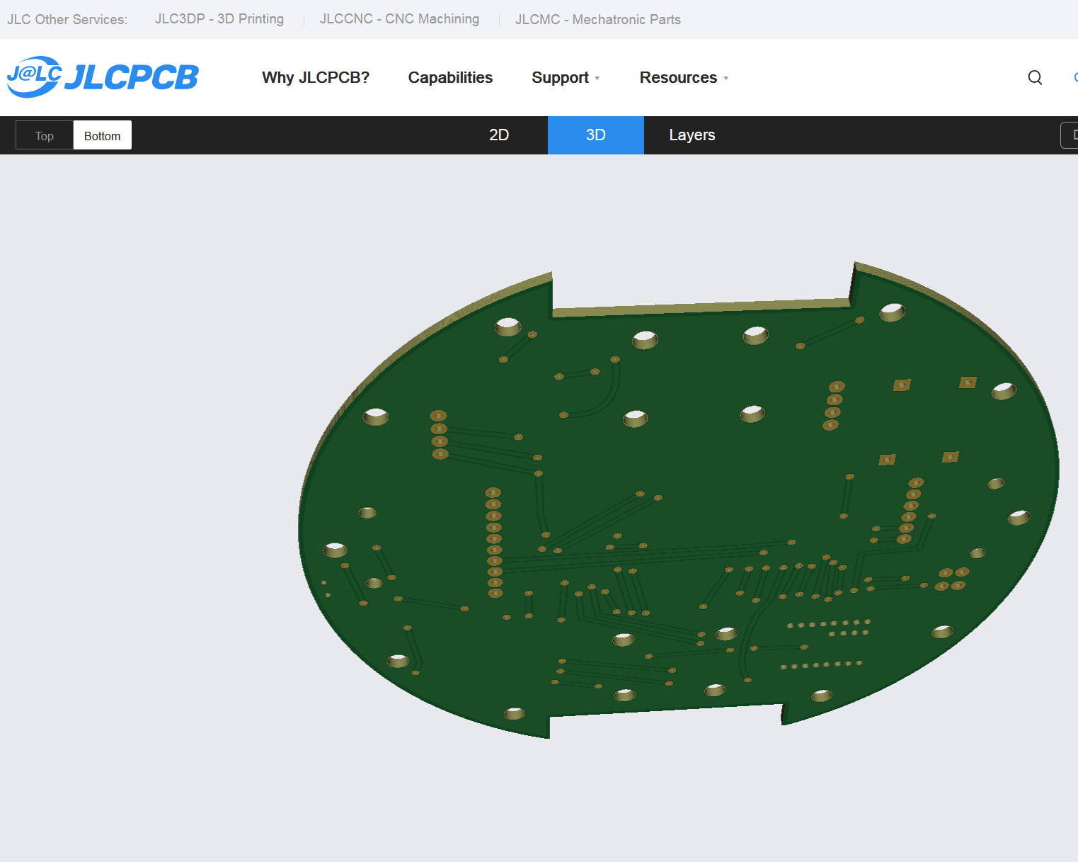
I downloaded the .svg and replaced the one in my fritzing file, exported as gerber folder, uploaded to pcb manufacturer, and the file is as expected thanks for helping.
I think the error I was making was the incorrect id label for the svg. I will be making more crazy shapes in future so it will be good practice to get right
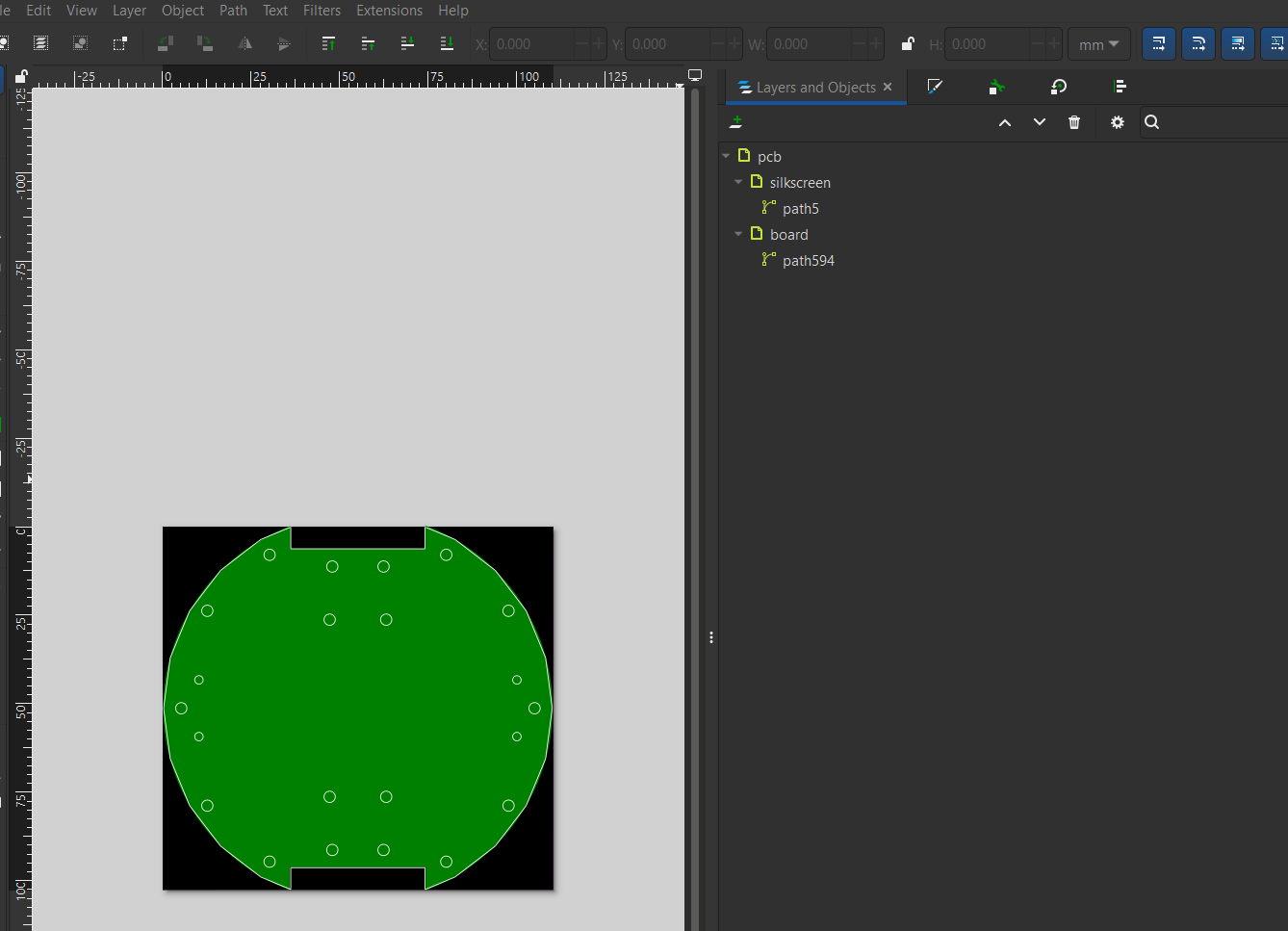
It has all the correct groups, labels, and values for the fill and stroke for the necessary svg. To make slots or holes you need a single differential path (there used to be an article telling you how to do that but I couldn’t find it when last I looked.) There are also various posts in the forums over the years a search for pcb slot should find them all.