had a go at laying out a PCB, Q: is there a way to add “guide” objects, rectangles, lines and similar. trying to lay out some sensors and need to get the spacing between them right and then the pairs of them in the correct space to interface with the other physical hardware.
ended up resorting to pencil and paper to work out the positioning, wondering if there is an easier way I’ve missed?
note not thinking things to appear on the eventual PCB, just pure graphical objects that can be sized an positioned - here to represent some third party hardware I need to work with
Not really, a few things that may help: the rulers (at the bottom of the core parts window) can be dragged around and won’t appear on the pcb. Vias can be positioned by changing their coords in Inspector, traces between them will produce shapes. You would need to delete them and the associated traces when the pcb is finished otherwise they will appear on the pcb. What I would probably do is use Inkscape to make an svg of the outlines and placements that you need and then import that as a silkscreen image. The svg editors are more suited to what you want than Fritzing. The problem may be getting rid of the silkscreen image when the board is complete though (I don’t know if there is a way other than editing the files to delete a silkscreen image, but editing the .fz file should do it as that is what loads it.) Easiest of all may be to make a custom part with the shape you need and insert that in the sketch, and delete it later. That would require learning to create parts though and that isn’t an easy subject.
Here is a part and associated pcb svg which has only the silkscreen layer represented by the pcb svg (currently a square made up of 4 lines.) Using the attached svg you can make changes as desired in the svg using Inkscape or another svg editor and then load it in to a new part using the parts editor or unzip the fzpz file, change the svg and rezip it (the group needs to remain silkscreen as at present for it to work):
Turns out the forum can’t upload the svg, so you will need to unzip the .fzpz file and modify
svg.pcb.silk-only_1_pcb.svg
to do what you need and then rezip the .fzpz file. SVGs will do much finer resolutions that .5mm, I’ve done footprints with less than 8 thou clearance on pads successfully (and finer is possible, the cheap board houses typically don’t go below 8 thou.)
In my current project, I am using an assortment of breakout boards and electronic components. I want everything to fit inside a specific case, so I’ve been doing the ‘fitment’ of the parts in CAD software. I’m using FreeCAD for that part, using rough, but accurate, shapes of the breakout boads. Mounting holes for the breakout boards are created in the CAD pcb board. Once I get everything to fit, I’ll output the pcd board as a svg file and load into fritizing. That way I will have to mounting holes to use as reference when placing parts in pcb view.
If you are more of a pencil & paper tyoe of guy, then using an svg editor would be the better choice. You can create squares and circles, and other shapes, to exact sizes. Inkscape isn’t that hard to learn, if you’ve ever used a paint program before, you’ll find it easy but different.
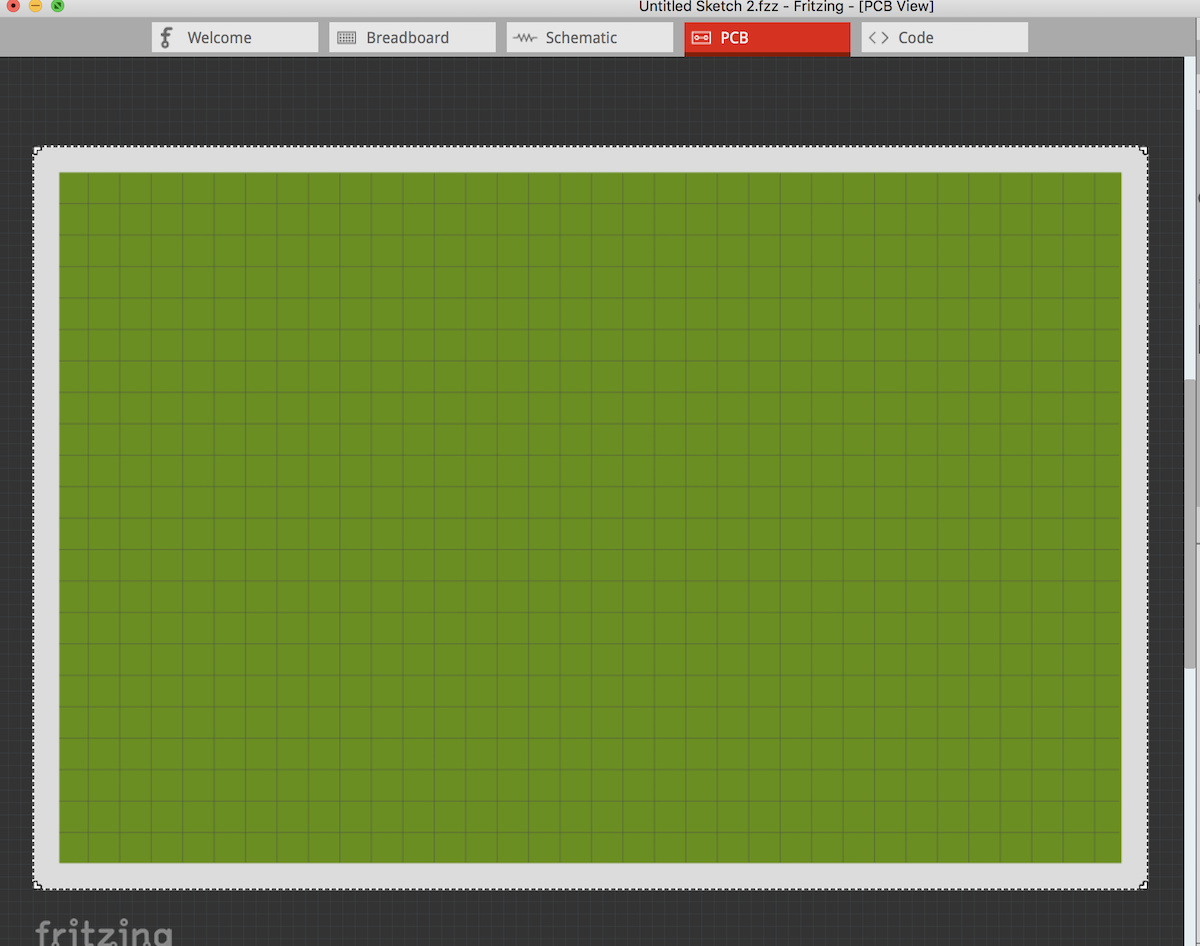
• Create a PCB svg with a grid on the Silkscreen (screenshot below with green pcb).
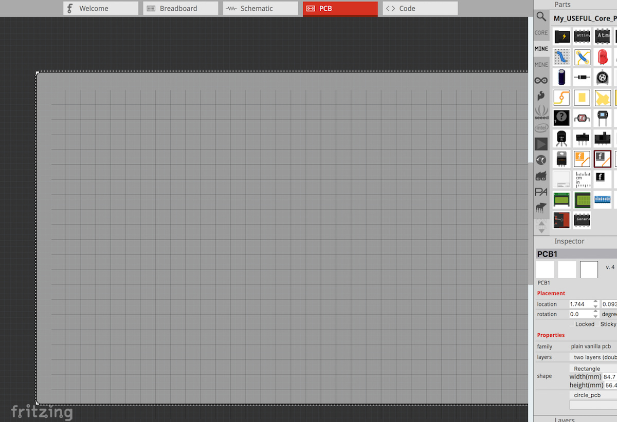
• Create Graphic svg with just the grid (screenshot below with a default grey pcb). The grid-graphic is loaded into a “Part” called Silkscreen Image.