PC817 Optocoupler

But again why are you assuming the part is the wrong size? From what I checked the file is the correct size so when is it you are seeing something wrong?

If you are only looking at Inkscape, then that’s normal. Inkscape always saves in px, the other units in the gui are translated from px. By default it starts and displays in px as well. Does the Fritzing part not work in some manner? If so post the part (7th button from the left in the reply tool bar) and one of us will have a look at it and tell you what is wrong.

Peter

The pads look too big in fritzing.

part

I assume that is a rendering from Ailser and what you are seeing around the pads is the solder resist making it look larger than it is. Check the copper only layer or as Vanepp said upload the part or sketch so we can check it out.

I’m using the original sketch. just changing the PCB graphic which I uploaded.

First SMT variant

Sharp PC817.fzpz (13.3 KB)

I played with your SVG awhile and could never find the exact reason it was scaling wrong. I found many places it had transforms and viewbox scaling, some in inches some in metric some in px etc which implies to me that you edited an existing svg to make this one and from my experience that almost never goes well.

So I tried remaking your svg as it is only 5 squares and 1 circle and it worked the first time.

drawing you will have to assign the connections in the parts editor as they are not defined in the svg.

Or try this one I exported from Fritzing.
Sharp PC817.fzpz (13.9 KB)

I should say also my inkscape is always in MM and my svg dimensions in Inkscape show as mm no px. When I open a new project in Inkscape it shows mm everywhere.


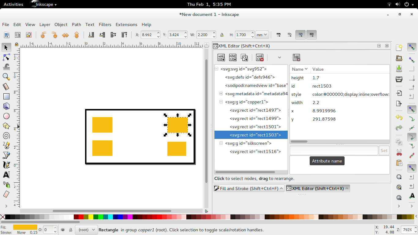
As you can see in the xml editor on the right the height is 1.7 which is mm and the width is 2.2 which is also the correct mm. Not px.

To set up your Inkscape like mine check this thread.

I should also add to my tips and tricks to always start a new drawing yourself and not to try and alter existing svgs unless you have parts creation down pat already.

Awesome, thanks. I did import stuff from another svg. I’m new to all this. I didn’t realize there were so many constants.

I guess I have to do a new part file and pcb.svg for each PCB layout?

For each new part footprint you create not each new pcb you make. But most parts out there have an equivalent footprint available and in that case you would only be changing labels. Like recently someone was looking for an Atmega1284 tqfp which is not in Fritzing but if you search for tqfp you will find some other part with a different name. In that case you open the part you found in the editor, save as a new part and change all the names and labels but leave the SVGs as they are (with the possible exception of the schematic which you may want to change the labels in the SVG). This is the case with most footprints you will be looking for. In your case there are no easy to find SMD gul wing 4 pad parts existing so making your own SVG was the only solution.

I do not believe you did anything wrong simply that each time you edit an SVG it gets more transforms and if someone else made the SVG it could have had the wrong PPI so they then scaled it and then you edit it and use the correct PPI but their scaling now makes yours wrong etc.

I just edited the footprint you fixed and have the wide SMT version also now.

I may be able to use an existing footprint for the THT footprint.

I’ll upload them all when I’m done. You guys are very helpful here. Good show.

@Troy1967 No problem we are here to help. When you know the SVG is clean or you created it yourself I think editing it is ok.

If you check the SVG i uploaded http://forum.fritzing.org/uploads/default/original/2X/9/95c85f93f54554dfb087e07e32e0a36f756cb0af.svg you will see each pad size is 1.7 by 2.2 which is mm so I do not believe you are correct that is always saves in px. The location is in px but not the size. If you start with a fresh SVG and have all the settings for the document set to mm the results are mm. If you start with an existing part it will be however the existing part was which I believe is one of the reasons they turn out wrong so often. I haven’t had issues since starting from scratch.

 <rect
       y="291.87598"
       x="8.9919996"
       height="1.7"
       width="2.2"
       id="rect1503"
       style="color:#000000;display:inline;overflow:visible;visibility:visible;opacity:1;fill:#f7bd13;fill-opacity:1;fill-rule:nonzero;stroke:none;stroke-width:0.15000004;stroke-miterlimit:4;stroke-dasharray:none;stroke-opacity:1;marker:none;enable-background:accumulate" />
  </g>

You will also see in the SVG header it has mm

   height="6mm"
   width="12mm">

That could well be correct, I never have figured out exactly what it saves in. Many things are always px (I believe due to CSS) but you may well be correct it depends on something (and I don’t know what something is) for what it saves in. I have also discovered it appears to be impossible to remove transforms from polygons automatically. None of the suggested fixes on line appear to work. The only success I have had is delete the transform with xml editor then edit the points again using xml editor to change the polygon (or polyline in this case) back to where it should be. That said progress is occurring. The above polyline came about in fixing the parts factory to output a correctly scaled schematic for headers. The current one (which I hadn’t noticed before) is scaled at .75 rather than the correct 10.41667 for 1px = 1 thou as the rest of the files are. I expect that is because of the issue of changing the polyline (since schematic is the only one not done). I just downloaded QT and Visual Studio to produce a head version on Windows as I have fixes for the two main file related annoyances (the crash and parts editor not deleting its files even when you tell it to).

Peter

So I just got a parts update and the PC817 is there with a through hole PCB layout. Wondering if someone smarter than me can just add these SMT layouts to it?

Optocoupler_PC817XFP_pcbOptocoupler_PC817XI_pcb

The only way to add to the core parts is to make a submission through Fritzings Part Repo on Github. Unless you are familiar with Github I would suggest for now you should just create your own parts and it will be in your “mine” parts bin for future use. You can also export those parts and upload them here to share with others looking for them.

If you are interested in learning how to submit a part to the core parts please read the following.

I have to learn how to make one part have multiple pcb layouts first.

At present in general you can’t. The ones that appear to do that in inspector are actually each individual parts with code in the source (which you can sometimes fool to add your parts) that does the selection between the parts.

Peter

Maybe I am not understanding what you are saying but if you open a part in the parts editor and go the metadata tab and make sure each part has the same family name and a different variant name you do get a part with different variants in the inspector under the variant field. Or at least when I have added to an existing family like the ESP8266 it has shown up in the variant field. I also used a test point as the base to create exposed copper artwork and the test point now shows 51 variants, oops (I should give them their own family).

yep I know that, what I meant (but obviously didn’t get across) is that some things such as changing the color bands on resistors are meant to be internal, but if you manipulate the fzp meta data (outside of parts editor which strips the important bits) you can sometimes convince Fritzing to apply the internal magic to your part that isn’t part of core.

Peter

Check in the main window when you are using the selection tool you can also set the units to mm (or inches) at the top where you adjust the location and dimensions of an object. Once you have set those can you confirm they are the right dimensions? I get 2.2mm x 1.7mm for each pad and they are [8.2mm] apart which is correct according to the datasheet

While that is true for a single sketch, that will not modify the underlying part (which is what was under discussion here.) To do that you need to edit the svg files which is a lot more complex.

Peter