I try to use older parts, especially elco’s are larger than new ones, and the pin distance then does not fit. I have tried to insert single jumper pins instead.
Is there an easy way to enlarge pin distance for elco’s and resistors?
Hello,
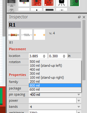
Did you tried inspector window…
There are more “Pin spacing/ package” option available…
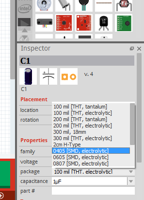
Thanks Blue, there is indeed more than met my eye at first; still, a 5W resistor in a ceramic jacket would need 1000 mil (25 mm). I also need to place a large elco with 44 mm spacing…!
Most likely the generic parts won’t work for those two, you would need a custom part. If you post a data sheet for the parts I’ll take a look (a 2 pin part is relatively trivial to make if you know part creation, less so if you don’t.) If all you need is PCB it can be done by dragging in a hole from core parts and then using Inspector to set the hole size and pad size suitably (although that won’t show in breadboard or schematic.)
Peter
Whenever I found a new part, I always create it for FZ for future…
But, I don’t have 1000mil res. Have 3cm & 2cm…
Here the 2 parts of mine for 5W res, check if they help…
81. Resistor 5W (ceramic).fzpz (4.6 KB)
82. Resistor 5W (wirewound).fzpz (5.7 KB)
** For the wirewound res, I make the hole as ellipse, because I found many of them doesn’t follow standard pin spacing…
Unfortunately ellipses don’t work in pcb. Your part generates no holes in the gerber output:
; NON-PLATED HOLES START AT T1
; THROUGH (PLATED) HOLES START AT T100
M48
INCH
%
T00
M30
so there will be no holes in the board. You need to put two circular pads overlaying the edge of the path so that the gerber drill.txt file will have plated through holes (which will require a dremel or a file to make an ellipse.) I can modify it if you like, but I expect you can do it for yourself.
Peter
1 Like
Oh… Thanks… I’ll update it…
I normally home etch…
Can you Please, check this part… If every pin showing error or not…
94. USB-A Female (Stand 90).fzpz (8.0 KB)
Then I’ve to update some other parts also before posting…
Well that took longer than it should have ![]() . It looks like you are using an older version of Illustrator that defaults to 72dpi and the svg dimensions are set to px rather than in. Fritzing (in this case anyway) dealt with that, but Inkscape isn’t as forgiving. I had to convert that svgs to the current 96dpi for Inkscape. I think setting dimensions to in should keep Illustrator happy too.
. It looks like you are using an older version of Illustrator that defaults to 72dpi and the svg dimensions are set to px rather than in. Fritzing (in this case anyway) dealt with that, but Inkscape isn’t as forgiving. I had to convert that svgs to the current 96dpi for Inkscape. I think setting dimensions to in should keep Illustrator happy too.
Here is the major problem, because of the path with no interior pads, the Fritzing gerber code generates no holes for the slot. To correct that I added 3 pads (only the bottom ones set as a connector), which I think the board houses may accept (I haven’t tried it but others say they have done similar things):
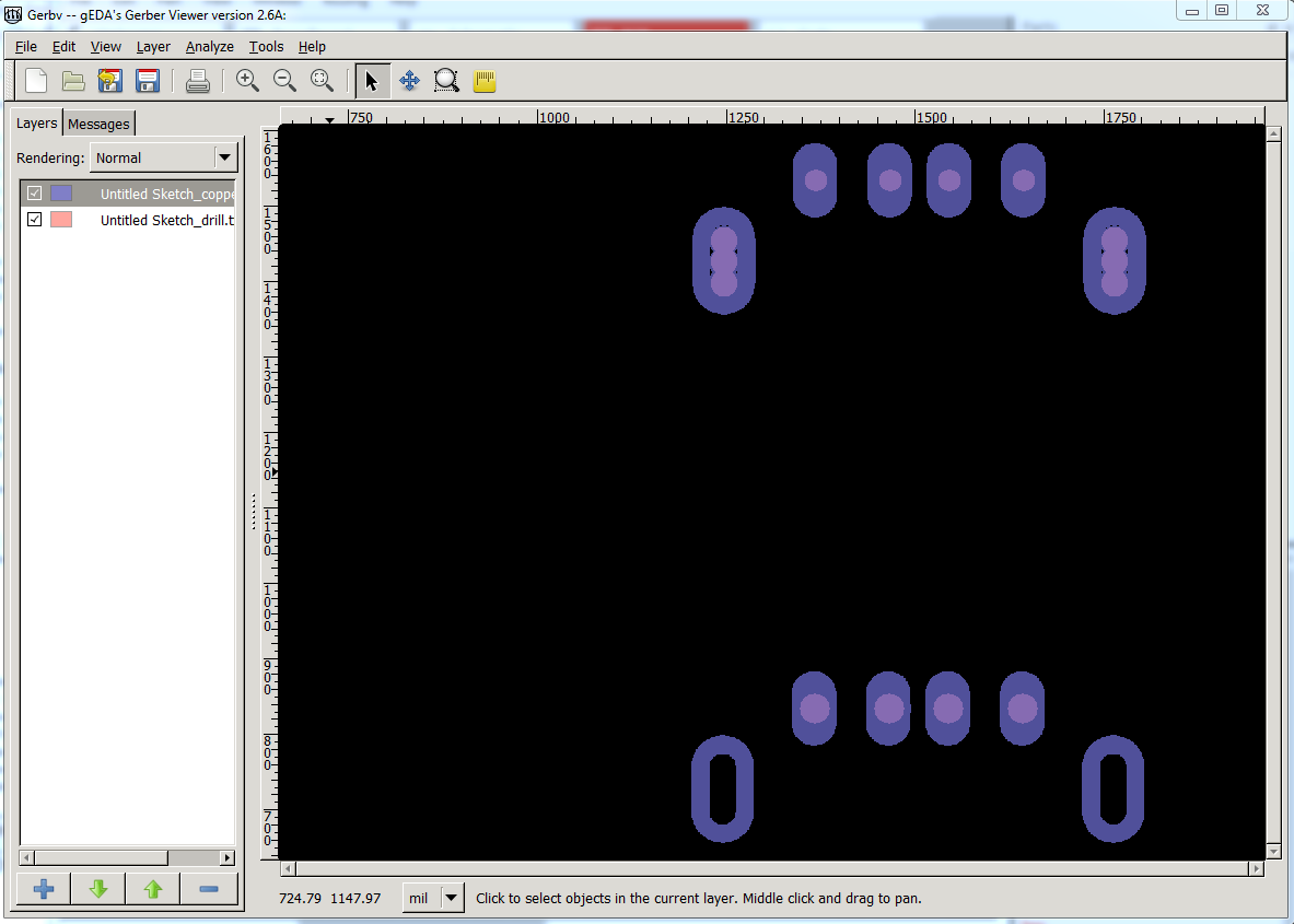
The top part is my fixed up one the bottom is the original. The lighter purple are the holes. As you see there are no holes in the slots of your part (and the pin holes look to be too large, in mine I reduced them to 0.03in as shown on a data sheet for a USB 3.0 through hole connector here:
https://www.mouser.ca/datasheet/2/670/uj3-ah-4-th-1313315.pdf
This produces this drill.txt file on geber export:
; NON-PLATED HOLES START AT T1
; THROUGH (PLATED) HOLES START AT T100
M48
INCH
T100C0.039500
T101C0.030000
T102C0.035667
%
T100
X017672Y014333
X018657Y014333
X019444Y014333
X020428Y014333
T101
X011460Y014333
X012444Y014333
X009688Y014333
X010672Y014333
T102
X013651Y012976
X013651Y013254
X013651Y013543
X008478Y012976
X008478Y013543
X008478Y013254
T00
M30
Which shows the 4 data pad holes ( T101C0.030000) as 0.03in plated through, and the 6 slot holes as 0.0395 (I probably should set that to 0.04in, which they will probably round up to anyway but I didn’t ![]() )
)
In all cases I re scaled the svgs so the internal units are in thousands of an inch. The procedure is detailed here:
At the same time I changed the scale from 72dpi to 96dpi and changed the units from px to in, so the dpi shouldn’t matter anymore. because of the units being in the svg should render at the same scale no matter the underlying dpi setting.
Breadboard
Pretty much identical except I renumbered the connectors in order starting at connector0
icon
I eliminated and reused breadboard. This saves the space of the icon svg.
pcb
rescaled, adjusted the size of the connector pads for the 4 data pins to make the holes be 0.03in, added similar pads (3 overlapping holes for each slot, with only the bottom one defined as a connector) to make holes for the slots. Changed the connector numbers to start at connector0 and match the pins in breadboard (it would be a good bet to check the resulting footprint against a real part to make sure I got it right!)
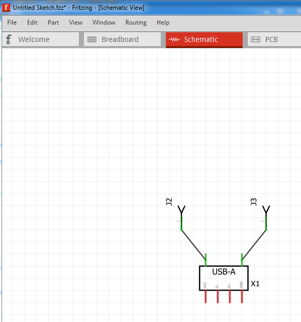
schematic
redid it entirely from the schematic template svg as that was easier. The 2 shield pins on your part’s schematic have either no or incorrectly placed terminalIds which cause the connection to the middle of the pin here (corrected in my part.)
and finally my corrected part:
94. USB-A Female (Stand 90)-fixed.fzpz (7.6 KB)
which has a modified moduleID and variant so it will load along side your original part for comparison.
Peter