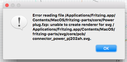
Thought I would try to edit the Power Plug in core parts. I must have done something wrong. The error messages I am getting are as follows:
My process was as follows:
Selected the power connector within the PCB layout.
Right click to Edit part.
In new part editor, selected part and went to show folder.
Opened in Inkscape.
Edited the XML code to change the “r” from 6000 to 2500.
Edited the XML code to change the stroke from 2000 to 1250.
Saved the file WITHOUT changing the filename. I thought this would be easier, because in the prior edits when I changed the part name, I could not find the new part, even though I was confident that the path and folders were accurate.
I closed Inkscape.
I closed the parts editor.
Selected the parts from the core parts again … and the error message occurred.
Questions … what did I do wrong.
How can I repopulate the core parts with the original file?
Why do I not see the “edited” version of the Inkscape file in the parts folder. Are separate files created for PCB and SCH and Breadboard … even if I edit just the PCB?
I have looked at the tutorials … and except for the creation of a zip file and extraction, I think I have not violated any basic editing guidelines.
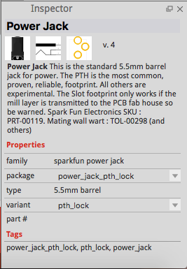
As an aside … it appears there is a version of the power connector that has smaller pins but they are not exactly as the spec sheet for the part I am using. It is called “sparkfun-connectors_power_jack_slot_pcb.svg”.
The following message is mentioned as a possible problem when using this power connector:
Would you please compare this or offer suggestions to which power connector image I should use to match the PJ-102AH power connector I am intending on using.
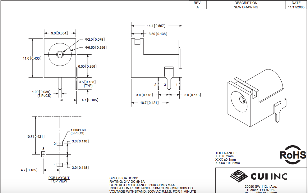
Here is the data specs for the PJ-102AH connector from Adafruit.
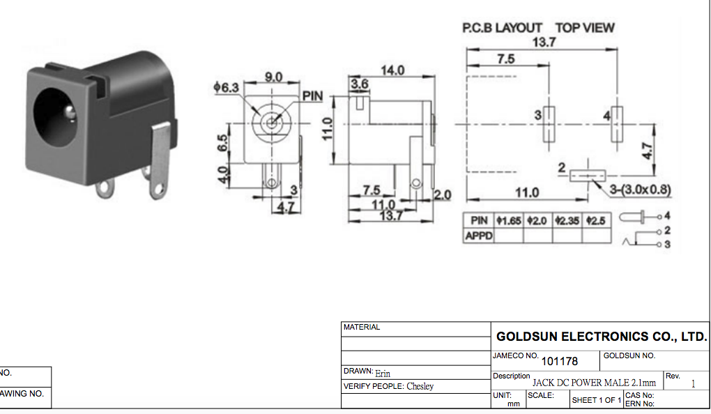
And here is yet another from Jameco Electronics:
This appears to match the larger holes that are the default “power connector” in the core parts bin. They are 3mm in diameter I believe.
There are a couple of possibilities, (its probably easiest to copy the refernced svg file somewhere then rename it from .svg to .fzpz and upload it here so we can have a look at it. Something is wrong in the svg which is breaking the fritzing renderer, by default Inkscape stores in Inkscape format and you are usually better to select “plain svg” in the file type menu. Its possible that something that Inkscape added is causing the problem. The next problems is that you shouldn’t modify the core parts directory as it is synced to the repository on github and thus when the next parts update is pushed your changes will be overwritten. The usual way to do this is to save as a new part in parts editor, then unzip, edit and rezip the files and use it as a new part.
I was just on my way out when I answered the first part of this question so now I’ll do this part (with the reminder that I’m not anywhere near a pcb expert ). First Fritzing doesn’t appear to create a mill layer gerber (at least not anything that says that or looks like it could be it in the gerber directory) so I suspect that needs something like eagle or kicad and thus likely isn’t an option for Fritzing. That said both the data sheets listed show the pin as being 3mm by 1mm and given that the only Fritzing option seems to be a hole, then as they say the pth option (which creates three 3mm or 0.118000in holes) seems like the best option and should fit any of the listed jacks. I expect that’s why they say that PTH is the best and most tested footprint option in the description. While it will have 2mm of space on the 1mm side of the pin, I expect (without having a board to try it in though) that it should be tight on the 3mm side of the pin and any less won’t fit. If you have access to a 3mm drill, I’d try and drill 3 3mm holes in a piece of fr4 and try the connector in them and see how well it fits.
Edit: followed my own advise a generic 2.5 mm barrel jack like the Jameco one with 3mm by 1mm slot, a piece of fr4 .1 pad per hole board and a 3mm drill bit in the drill press. Two 3mm holes at .25in apart and a third 3mm hole mid way between the first hole offset by .2in (the third pin on my jack is only 2.5mm not 3) and the jack fits fine. There is a little spare room but not overly much and I’ve drilled out the plating so a plated through hole would be tighter. Looks to me like the PHT foot print is as they say, the correct one to use. As a bonus (as mine are like the Jameco one with solder tabs) there is enough room to put a resistor wire through the tab on the bottom of the board to give it additional mechanical strength if you like.