Part update breaking existing connections in breadboard and pcb views

Testing the update process for a part being obsoleted worked with a simplified test sketch, but a slightly more realistic sketch lost connections and traces in the pcb. There was a bit of minor cleanup needed on the breadboard view, that amounted to moving breadboard and updated part slightly to get them to reconnect. Schematic view updated fine.

@vanepp I figured this belonged in its own topic. Probably nothing to do with property names :slight_smile:

The sample drawing and update were done using Fritzing 0.9.4b commit c595162a1d0 on a full up to date Fedora 31 workstation.

Here is what the pcb view looks like before the led matrix part is obsoleted. Don’t try to make sense of that as normal pcb. This was for an experiment to mount the controller chip directly on the back of the led matrix, and use direct point to point wirewraping instead of pcp traces. This just provides a visual tool for planning the wirewrap connections. Though I was pleased to find I could layout the pcb with only a single via.

Here is what it looks like after the part was obsoleted, the sketch reloaded, and the part updated. All connections are now ratsnest lines, and many of the traces (especially top) are missing. Others are missing from some of the bend points.

Here is what it looks like with the led matrix part moved left 0.1 inch and down 0.2 inches, showing that the traces that remain are not actually connected to the part.

Attached is the drawing, from before the update was done. To replicate the steps, you will need to use the 8x8_led_matrix branch of my fritzing-parts repository. That is where both the new parts, and the obsolete LBT2088ah part exist.

LBT2088AH test.fzz (28.0 KB)

git clone https://github.com/mMerlin/fritzing-parts.git --branch 8x8_led_matrix

Anyone have ideas on what would cause that sort of breakage, when both the new and obsoleted part have been shown to work in a simpler drawing?

test-orig-master.fzz (8.7 KB)

Extra information. Many of the open ended circuit traces only partly exist. Trying to move the end point, or add a bend point causes them to vanish. The board design was done in the schematic view, except for JP1. That was connected after most of the pcb board routing was finished, and it became obvious which connections would most easily reach which pin. There isn’t really a molex connector there. Just a bundle of wires going off board.

Fixed. There are a couple of problems. Started from the original sketch and said no to upgrade. Align to grid is off in breadboard and pcb. Enabled it in both of them. Tried changing the breadboards from tiny to half, and ran in to a bug where the breadboards don’t swap correctly (likely because of different pin numbering). Marked that on my bug list, and went for plan B: moved the current breadboards down and up a bit to make the connections more visible. In pcb set align to grid on, unlocked and moved all (or most) of the parts so they align to the grid then locked them again. That breaks DRC, because the between pad runs are too close with the 0.05in grid size, so reduce that to 0.01in and moved the through pad traces til DRC passes. Save that here:

LBT2088AH-test-new-breadboard.fzz (28.4 KB)

Now exited Fritzing then restarted and reloaded the above .fzz file and said yes to replace. Now breadboard is correct without change (likely due to align to grid), as is schematic after straightening the lines for the reduced pin alignment. Pcb is more messed up. So View disable rats nest lines so as to not create connections from the rats nest lines. Then move the end of the unconnected wires back and forward on to the associated pad to remake the connection and all reconnects correctly and DRC passes.

LBT2088AH-test-new-breadboard-fixed.fzz (28.2 KB)

come to think of it rats nest in pcb is probably still off in this …

Peter

I had both forgotten I had turned that off, and did not know it would cause problems when updating the part. I turned it off on the breadboard view, so I could get the led matrix pins to align to the 2 separate breadboards. Turning the alignment grid size down as you did is another option. On the pcb, as you discovered, the space for the traces is tight, so again I turned of the grid alignment to gain (zoomed in) positioning freedom. I’ll have to adjust my process to use small grid spacing instead.

Also, that needs to go into usage documentation. If minor alignment / positioning differences are going to break part updating. Both as a strong recommendation to keep aligned to grid, and as a step to try if updating parts breaks things.

It is very hard to setup a breadboard numbering sequence that does not break when the size changes. Because the total number of pins changes, and the rule is that they are supposed to stay sequential.

If we could start at zero for the groups of five, and increment enough to handle the largest breadboard, then skip ahead to a convenient number (say 1000), and start a new sequence for the side connections, jumping by 100 for each group, then they should all be able to stay lined up. Otherwise you need a breadboard to breadboard pin mapping, similar to what is used for updating obsoleted parts.

Normally I would say you need that mapping for every breadboard, to every other breadboard. But, mapping each breadboard to that theoretical breadboard, matching the numbering pattern suggested above with gaps, would allow a 2 step mapping to work. So, define a fake breadboard with 200 groups of 5, and 8 groups of 100 (to handle the breadboards with the split in the middle of the side groups), with numbering from 0 to 1799, and map the connections of every real breadboard to that. That mapping could be shortcut drastically, if there was a way to specify the start and length of a sequential sequence. For the half+ breadboard, map
0 to 0, and continue for 150 entries, map 150 to 500, and continue for 150 entries, map 300 to 1000 and continue for 25 entries, map 325 to 1100 and continue for 25 entries, map 350 to 1200 and continue for 25 entries, map 375 to 1300 and continue for 25 entries. That would be a lot shorter than doing 400 pin mapping entries. Because the pattern is consistent that could even be reduced to just [0, 150, 300, -1, 325, -1, 350, -1, 375, -1], specifying the starting connection number for each connected group (of groups), with “-1” because the side groups are not split. With the right code, [150, 25, -1] is enough.

To improve that, might need an offset value, for how far the side groups are offset from the 0 row. Though simple centering should be very close (and a pain when that does not land on the 0.1 inch grid).

That can be used to match pins of a breadboard to any larger breadboard (up to 100 rows long). The other direction, there will be some truncation. Bonus if you (user) can specify an offset, so the middle of the bigger breadboard maps to the smaller one, instead of starting from the end.

Same kind of issues with strip boards, but I don’t think a general solution is possible for them. There are too many different connection patterns to create a general mapping.

I didn’t know that it would help, just that it couldn’t hurt :slight_smile: . Some of the breadboards are slightly misaligned (on my list of things to fix) by not being exactly on .1 boundaries. It may be that the wire reconnect is depending on the snap to grid function (or may not :slight_smile: ) which is why I tried it. I moved the breadboards because I seemed to be having trouble getting both sides to sync at once (one side or the other would but not both) indicating an alignment problem. Moving them didn’t snap to a grid leading me to check that.

No disagreement there, although first we need to find someone willing to write and capable of writing usage documentation :slight_smile: and as usual someone hasn’t appeared yet.

They are set up in groups now (there are potentially problems with some of the odd ones I have made for people over the years, there are some with 6 pins per row for instance.) The issue was the wires already connected to the breadboard when I resized it, so perhaps the answer will be “don’t have wires on the breadboard when you resize it” because sometimes (larger breadboard to smaller for instance) that just can’t work. I think with some thought the smaller to larger could work, something to consider when I get around to the clean up core parts project (breadboard pin alignment and normalization because most of the setups are a bit different) are on the list.

Peter

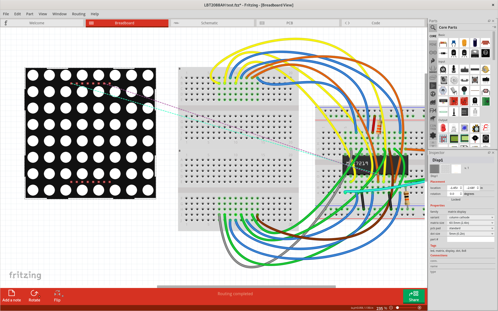
I think the pin rows of the original part were not an exact multiple of .1 inch apart. Which was why I had to initially fiddle with the breadboard positioning to get things to connect. Then the new part was at exactly 1800mils row spacing (if I did it correctly), so needed to fiddle with the positioning again. Though simply turning snap back on, and jiggling the breadboards would probably have got back in alignment.

Confirmed that with 2 “tiny” breadboards positioned at exactly 1.5 inch vertical offset, that the new 60mm LED Matrix part connects with no issues. Whether the align to grid is on or off. Tested by having align turned on, grid size 0.1, positioning the breadboards, locking the breadboards, then positioning the LED matrix both with align to grid turned off and on.

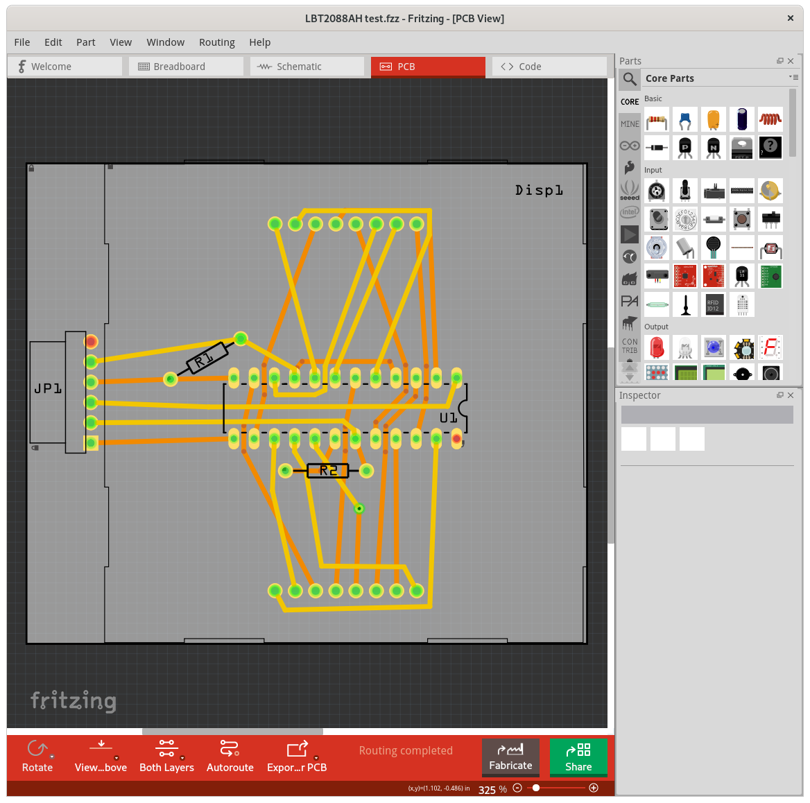
However, I just retested from scratch using the existing master branch and old LBT2088AH part. It too connected just fine, with or without align to grid, when the “tiny” breadboards were positioned and locked at 1.5 inch separation.

Back to my copy of the “LBT2088AH test.fzz” file, turn on align to grid, grid size .1, tweak the breadboard position to snap to grid, lock them, move the part off, then back on the breadboard, connects with no problems. Easily with align to grid on, a little fussy when turned off.

I probably turned it off exploring where to position the resistors. The side bus connections on the “half+” breadboard I use are offset horizontally from the core groups. Apparently by .05 inch. That makes connecting a resistor from the ground or power bus to a pin in the center groups tricky. It will often snap to the wrong side. So turn align to grid off, and carefully position where it connects properly. Or rotate to one of ±84, ±96 degrees. That is cleanest, but can break the associated connection on the schematic view.

Next, I cleaned up that copy, replicating approximately what you did. Saved that, exited, switched parts libraries (actually just changed the checked out branch in that case), rebuilt the parts database, and did the update again. The breadboard view initially looks cleaner. A couple of bogus wires, and ratsnest lines, where a couple of the updated part pins did not reconnect to the breadboards.

Verify that align to grid is on, set to 0.1 in, then jiggle the LED matrix part takes care of the ratsnest lines, but also show a lot more bogus wires. Moving the part away from the breadboard shows.

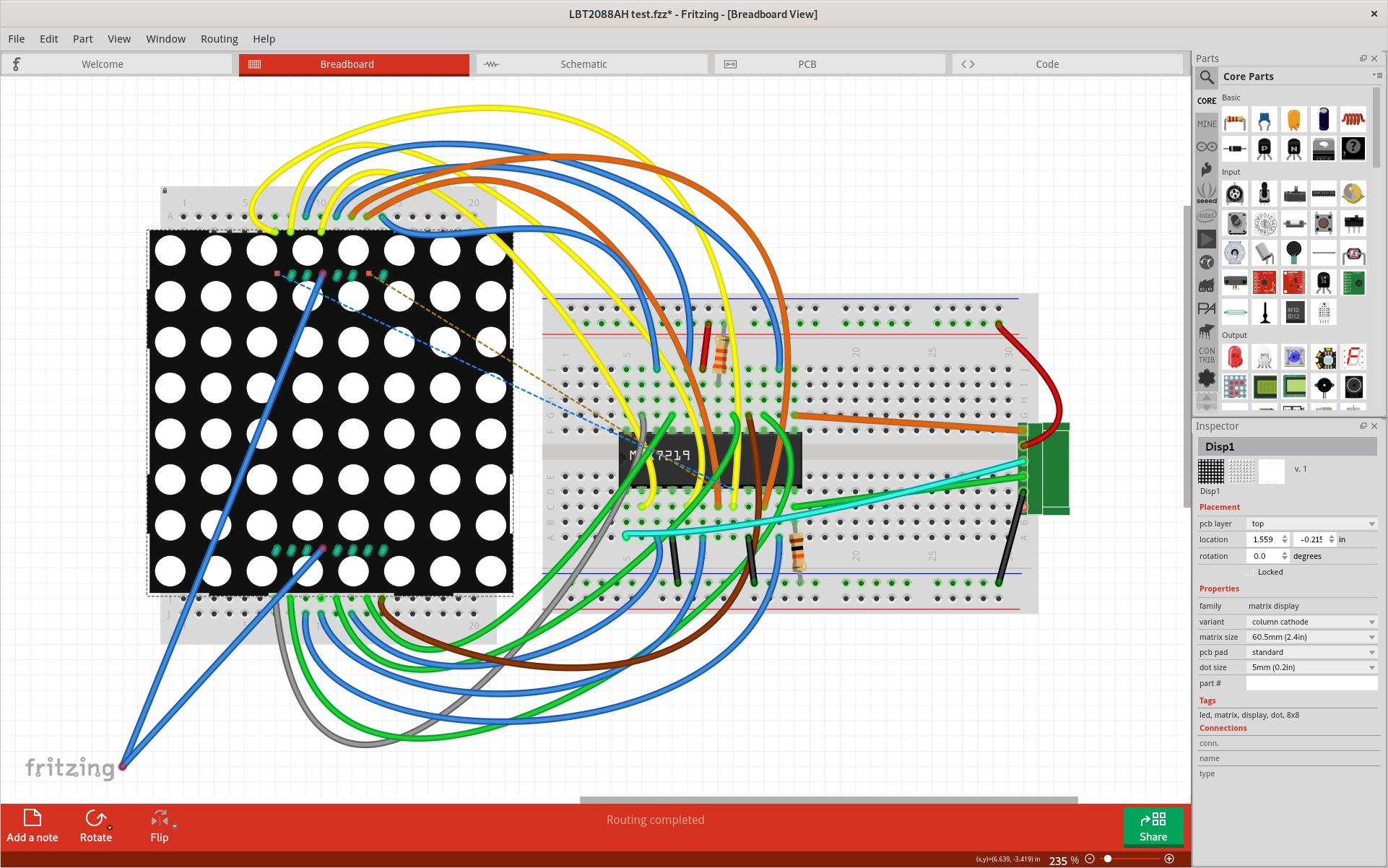
The initial ratsnest lines were actually the best part. A simple part move fixed them. Still not too bad. Just move the part away, delete the wires, and move it back. Or not. Deleting the wires did not create ratsnest lines. Checking the schematic view shows the connections all still in place. Moving the part back into position on the breadboards got rid of the 2 ratsnest lines again, and the breadboard view looks proper. But the pins are not really connected. Moving the matrix away from breadboard again still shows only the 2 ratsnest lines. Though schematic view looks just fine, and moving the part there drags all of the wire connections along with it. Pretty sure there is a bug in there someplace. Quite possible a nest of them.

2 pins did not connect at all on update (correctly) getting ratsnest lines to where they needed to go. 2 created bogus wires to nowhere, and the rest create bogus, almost zero length, wires where they should have just connected to the breadboard. The only pins that seem have really been connected (internal program circuit connections) were the 2 rats nest lines. Otherwise, deleting the wires should have converted to ratsnest lines.

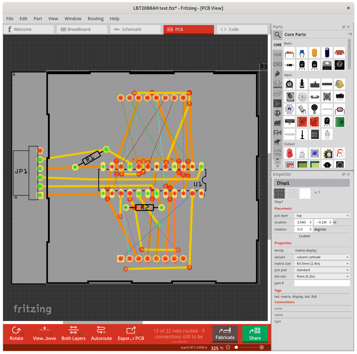
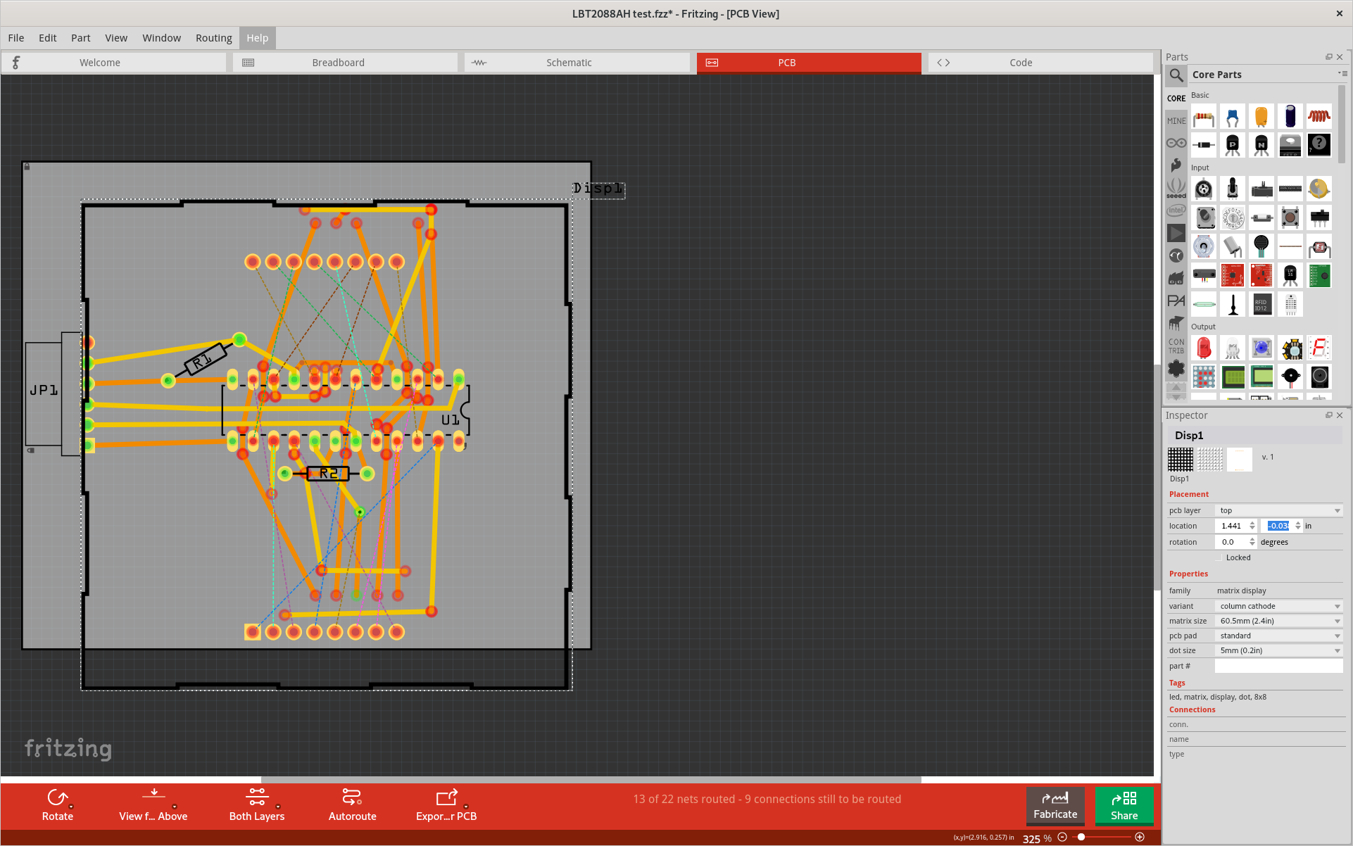
Opened your LBT2088AH-test-new-breadboard.fzz, visually saw the part move slightly on update. No visually bogus wires, or ratsnest lines, but moving the part off of the breadboards shows that all of the pins are connected to the breadboards with new wires. Deleting those wires did not create ratsnest lines. Schematic view has all of the proper connections. PCB view looks a bit better than mine, but there are a lot of red circles where traces are not connected to anything. Moving the matrix part shows that ALL of the top layer traces are disconnected. The bottom seems fine. That points to a possible copper0 / copper1 problem in the update process. Moving the part back into position did not reconnect. Moving the part away, to be able separate the connection pin and unconnected trace, I could move the open trace end and get it to reconnect. Move the part back where it belongs, and rules check passed too.

AND doing the fixes on the PCB view also brought back 5 more of the ratsnest lines on the breadboard view. 7 top layer traces were fix on PCB view. Checking pin numbers, it is all of the PCB top layer traces that have ratsnest lines on the breadboard view. 2 were there to start with.

I think we are going to need to see if we can create a (or several) smaller/simpler test case, to narrow down which conditions cause problems here. The update for LVT2088AH has to work hard on the connections. There are replacedBy keys all through it, and for several different reasons. That that all top layer traces failing is a good hint for one problem.

While I like my theory that all was well better, that does seem to be blown. I agee the thing to do now is find the minimal set of wires that cause the problem so that ubiquitous person someone can fix it (might even be you or I one day :slight_smile: .)

Peter

Bringing references over here for a work around.

work around discover
reimplementation and testing

The apparent cause of the bogus breadboard wires and disconnected pcb traces is a slight mismatch in the spacing of the connection pin rows between the new and old part in the breadboard view svg file. The new part is exactly 1800mils row spacing the old part was off a bit. The vertical px per inch calculation based on the svg height and viewBox was (172.129/2.39568) = 71.84975 px. Not quite the standard 72. The offset between the pin rows was (151.682-21.288) = 130.394px / (px/inch) = 1.8148 inches (1814.8mils). Changing the 151.682 coordinate values to 151.288 to get an even 130 px separation / (px/inch) = 1.8093 inches (1809.3mils). That was close enough to let the part update process finish properly, while not breaking any connections in the example existing sketch, if the update was not done.
If the scaling had been the expected 72 px/in, that would have been a change from 1811mils to 1805.6 mils.
With the viewBox scaling, 1.8 inches should really have been 129.33 px.