Part requires both copper top and bottom layers?

I wonder if anyone can help clarify the cause of the following problem with a part I created (
MT3608 Module.fzpz (31.1 KB)).

The intent was for the [top] copper layer to appear as shown:

MT3608 pcb

with regular PTH connections, but with ‘enlarged’ pads.

When attempting to create a PCB to support this module, Fritzing reports the following for each of the 4 pins of the module when performing the DRC:

Part MT3608 Module ‘M1’ is overlapping (top layer)
Connector Pin1 on Part MT3608 Module ‘M1’ should have both copper top and bottom layers, but the svg only specifies one layer

I can probably reason why the part components are reported as overlapping. The part effectively includes ‘pads’ around the pin holes in the top copper layer [as separate elements], but there was no intent to include these pads on both sides of the PCB.

The part file includes both copper0 and copper1 layers, but everything [in the svg] is indeed defined on just one layer.

Should I have done things differently?

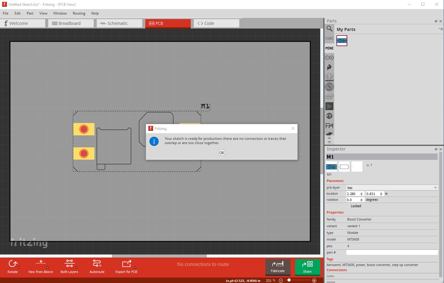
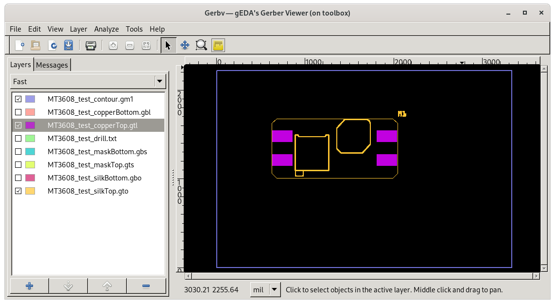
The fzp has both copper0 and copper1 defined, which is needed for a THT part. So the pcb needs both as well. To get something on one side but not the other, it needs to be in only one of those 2 groups. The fix here is to change the inner “copper0_1_” group to just “copper0”. That gets the 2 groups to match what the fzp says. To get the extended pads on only one side, move them from inside the «renamed» copper0 group, to just the copper1 group.

  <g
    id="copper1"
    gorn="0.2">
    <path
      fill="#FFBD00"
      d="M0.723,29.392v8.788h15.874v-8.788H0.723z M8.66,36.868c-1.703,0-3.083-1.379-3.083-3.082s1.38-3.082,3.083-3.082s3.083,1.379,3.083,3.082S10.363,36.868,8.66,36.868z"
    />
    <path
      fill="#FFBD00"
      d="M0.723,10.012v8.788h15.874v-8.788H0.723z M8.66,17.488c-1.703,0-3.083-1.38-3.083-3.083c0-1.702,1.38-3.082,3.083-3.082s3.083,1.38,3.083,3.082C11.743,16.108,10.363,17.488,8.66,17.488z"
    />
    <path
      fill="#FFBD00"
      d="M85.449,10.012v8.788h15.874v-8.788H85.449z M93.386,17.488c-1.702,0-3.082-1.38-3.082-3.083c0-1.702,1.38-3.082,3.082-3.082c1.703,0,3.083,1.38,3.083,3.082C96.469,16.108,95.089,17.488,93.386,17.488z"
    />
    <path
      fill="#FFBD00"
      d="M85.449,29.392v8.788h15.874v-8.788H85.449z M93.386,36.868c-1.702,0-3.082-1.379-3.082-3.082s1.38-3.082,3.082-3.082c1.703,0,3.083,1.379,3.083,3.082S95.089,36.868,93.386,36.868z"
    />
    <g
      id="copper0"
      gorn="0.2.0">
      <circle
…

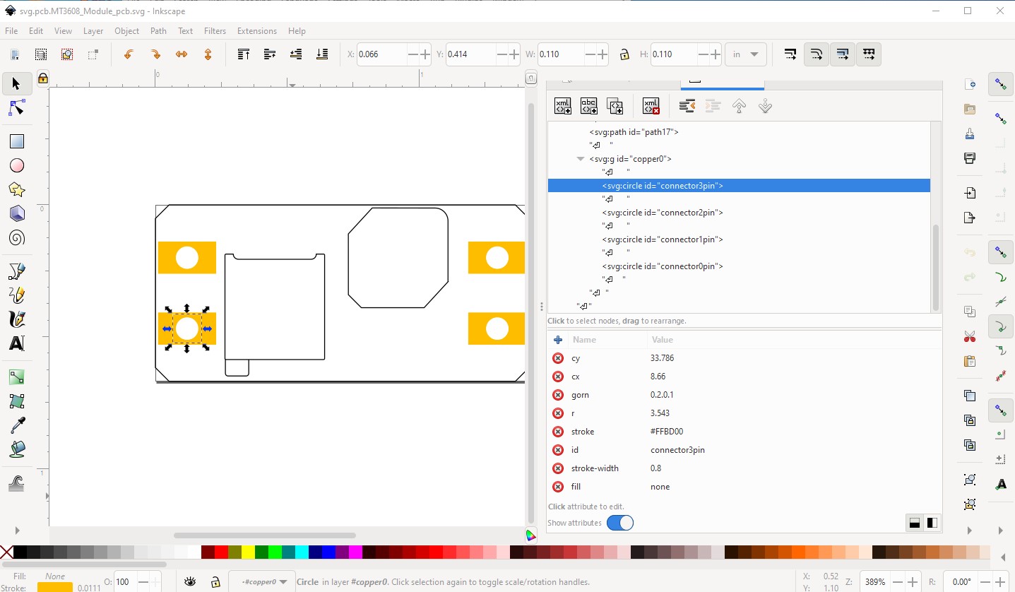
I edited the svg files manually (text editor), but the same is possible with inkscape or Illustrator. Now the circle elements, which need to be on both sides, are all that is left in the copper0 group.

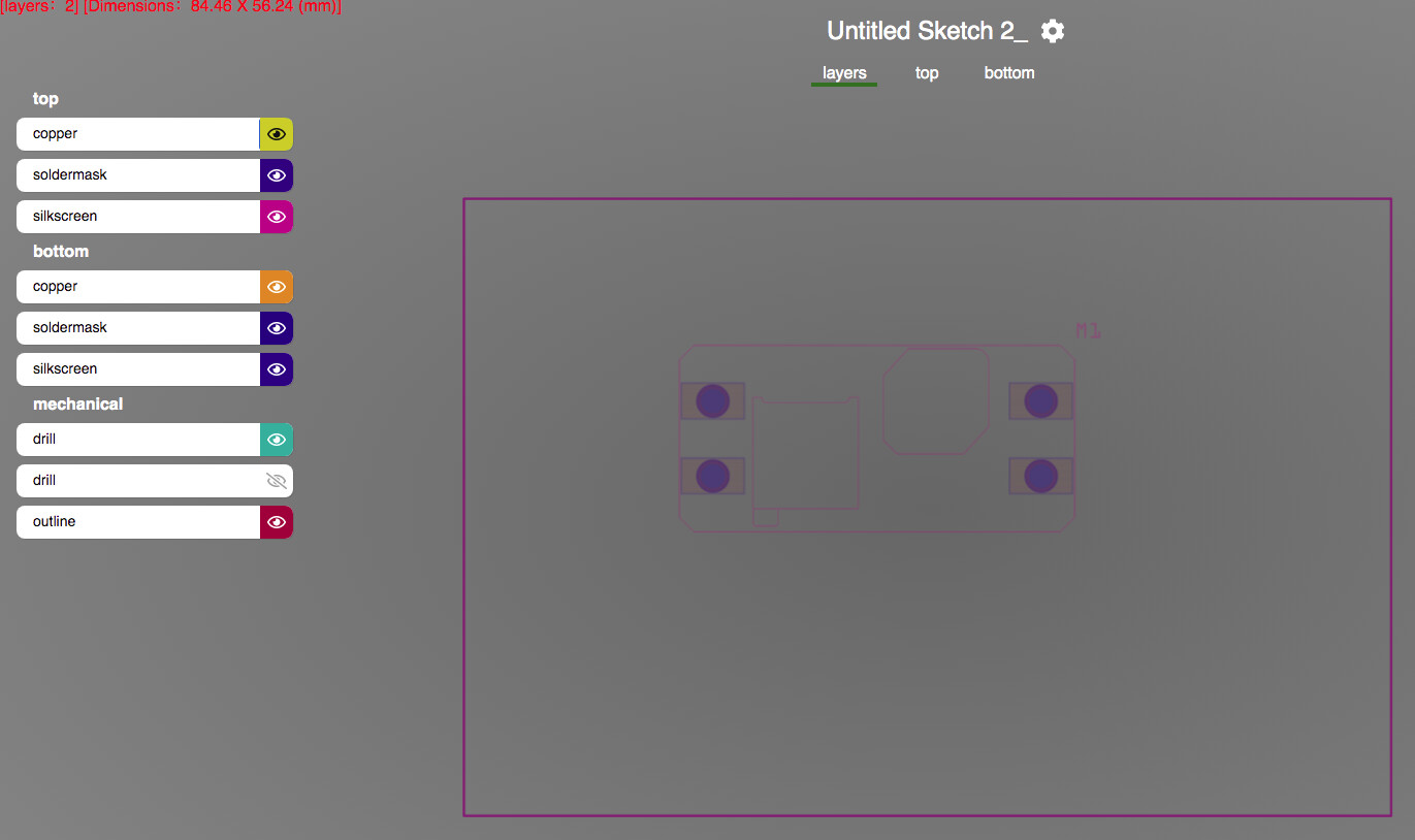
There is a separate problem with the breadboard and schematic svg files. At least according to FritzingCheckPart. You (or Illustrator) have the proper breadboard and schematic layer ids in the svg elements. I do not know if that works properly (did not test it), but FritzingCheckPart says those should be the id of a group. I created groups to wrap the content of everything after the desc elements, and moved the id those to keep FCP happy. I also added a “_test” suffix to the moduleId in the fzp file, so you can load this along side your existing part, to compare the difference in how Fritzing handles them. Here is my modified part, plus the pcb svg I used.

MT3608_Module_test.fzpz (30.9 KB)

svg.pcb.MT3608_Module_pcb

My only question is do you want the holes to be 0.087in? That seems a little large to me. A header is only 0.038in and a 1n4001 diode is 0.042in. That may be as intended though as it is about right for 14ga wire.

Peter

Yes, I just made the holes the same size as those in the module.

Everything seems to work now with @microMerlin’s fixes. I’m not sure I can see any way around the problem in general, which will probably be related to how Illustrator manages things, other than manually editing the svg file as has been done in the present case. I generally have to edit the svg file in any case to correct inevitable floating point variations with hole sizes.

I also regularly get the warning messages mentioned when running FCP, which are presumably yet again the result of the way Illustrator does things, but on previous advice I’ve never worried about them. They’ve not had any noticeable negative impact on anything I’ve done to date.

The ‘overlapping issue’ still seems to be there (still reported by DRC). Is that going to cause trouble somewhere down the track?

Doesn’t appear for me on Fritzing 0.9.9 on Win10:

with @microMerlin 's part above.

As an aside, I’m not sure the holes will be plated through without copper on the bottom of the board (I’m not sure they won’t be either as I have never done this!)

Peter

OK, good. I was using an older version (0.9.3) on an old Mac (that runs an old version of Illustrator that is not subject to subscription fees!) that I use for the design work.

There should be copper on the bottom from the standard circle element. The top is just getting “extra” copper to expand the pads.

Somethings wrong:

the bottom copper pads are misplaced which I had missed (I thought they weren’t there intentionally ). This would usually be translates but it doesn’t appear to be in this case. I think I would just put the larger pads on both sides of the board as being the easiest fix unless there is a reason for only wanting them on the top of the board. All looks well in Inkscape, but not in the gerber output.

Peter

Very odd. There is not so much as a single transform in the pcb svg. Nothing that should cause an offset. If I had done this from scratch myself, the paths would be a bit different. What is there looks valid. I dislike the mixing of absolute and relative coordinates like that, but there is nothing wrong.

I tried on my system:
5.14.18-100.fc33.x86_64
Flatpak 1.10.5
Fritzing org.fritzing.Fritzing 0.9.6 stable user
Fritzing Version 0.9.6 (b0.9.6 2021-02-21) 64 [Qt 5.15.3]

It works here.

As an extra test, I moved the copper1 path elements to after the copper0 group

<g id="copper1>
  <g id="copper0>
    …
  </g>
  <path …

MT3608_Module_test2.fzpz (30.9 KB)

That worked for me as well.

I think this is a bug in the greber export introduced in one of the most recent versions. My flatpack version is a bit older.

I just did an export from 0.9.3 and all seemed OK in the [arbitrary] Gerber viewer I located on the Web:

Yep, this was generated on Fritzing version 0.9.9. I too don’t see any problems in the xml.

Peter

I just generated the gerbers from 0.9.9 and they display exactly the same as my 0.9.3 export…

So maybe not a Fritzing bug at all. Or it is only in the Windows version. Maybe something unique in the environment @vanepp is using. Blame the gerber viewer? Though I think I am using the linux version of the same program.

gerbv version 2.7.0

I’m just using the first browser-based gerber viewer I found on the Web (https://www.elecrow.com/gerberviewer.html).

Some screw up here. I just reloaded your .fzpz and exported it and this time the export works fine. Don’t know why the first one screwed up though.

Peter