Someone in this post
Posted a part
At first glance, the part looks OK. However, it lacks a proper schematic layout.
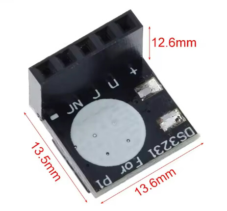
with the dimensions
Next I’ll redo @codeflsgruen’s part which is somewhat broken
First, start with this part (in the first link)
and unzip it. You will find the files for the respective views.
Breadboard SVG
First, download 2 files from
svg/headers/female/5-header.svg
svg/generic-button-battery.svg
Next, delete everything in the file
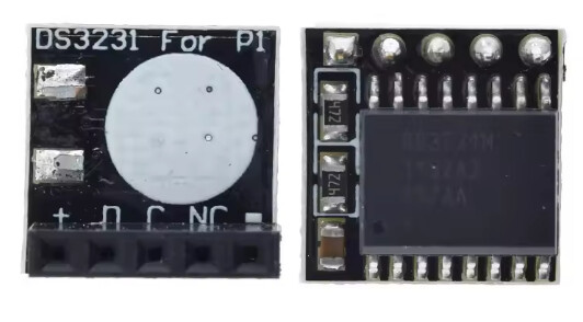
and import this image
into Fritzing
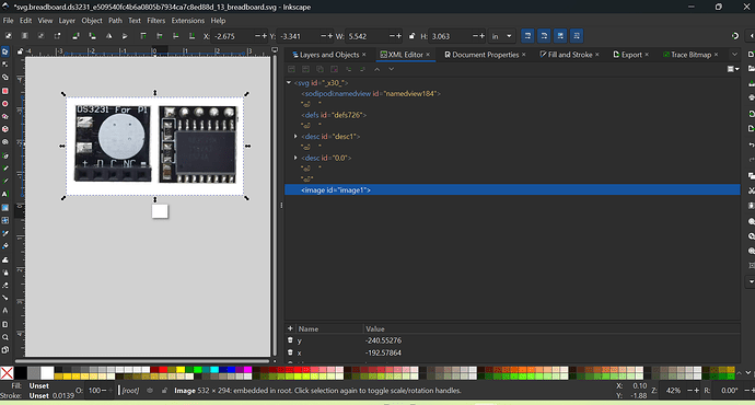
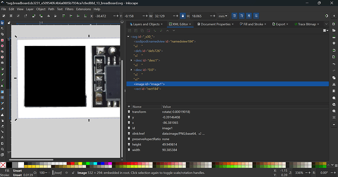
Obviously, It’s too big
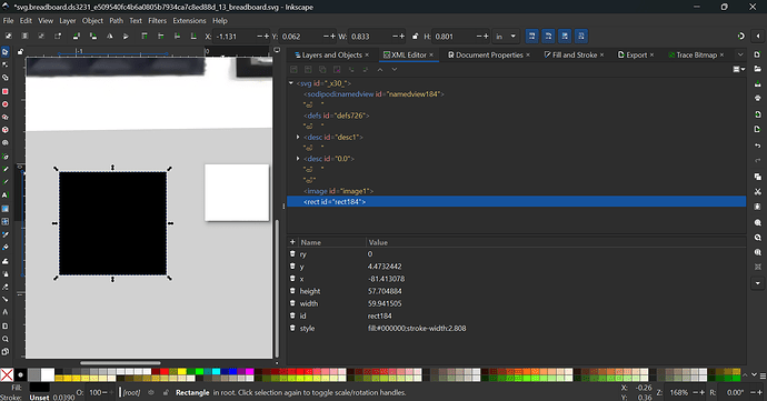
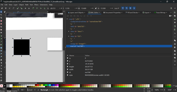
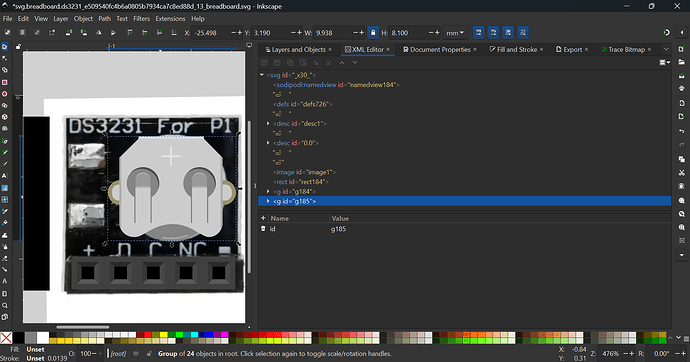
Next, rotate the image such that the board is straight and then create a random rectangle
Set the correct with and height
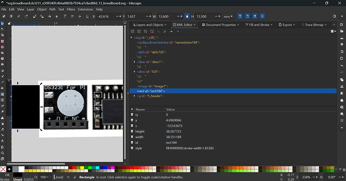
Scale the image
Next, move the rect away
Now we can start letting copy/paste do the work
First, add the headers
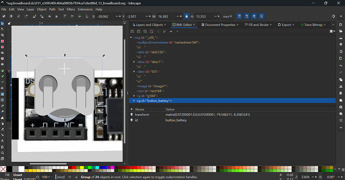
Then the battery
Too big, so make it smaller
Tip:
- Ungroup the groups to remove the transforms
- Layer the groups correctly – in any case, the headers must be at the topmost layer
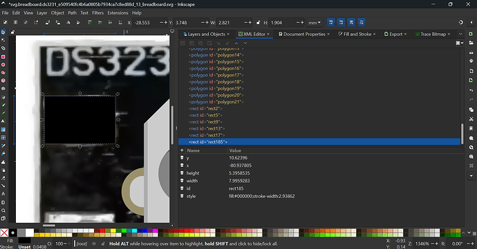
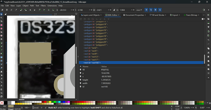
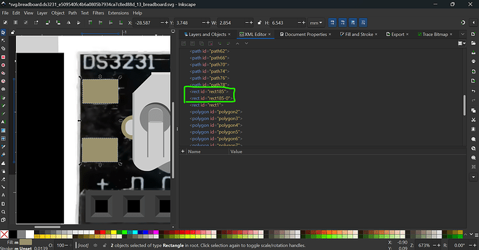
Next, create 2 rectangles with fill #9a916c.
change from the above to
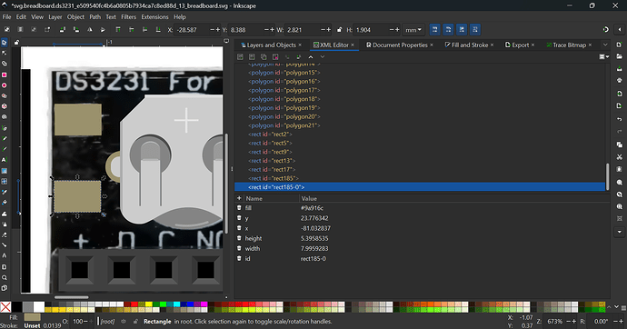
copy and paste the rectangle
Then bring them to before rect1.
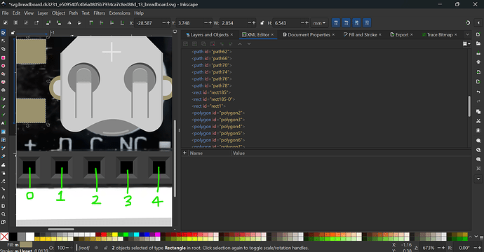
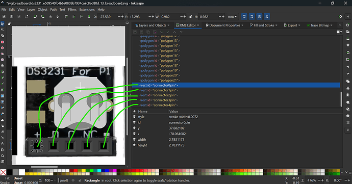
The next and final step – number the connectors.
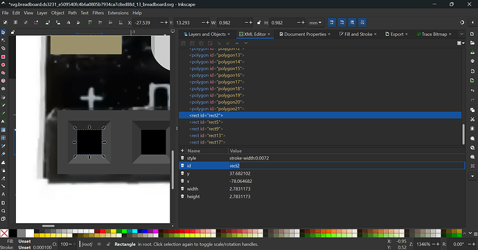
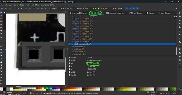
First, let the first connector be connector0pin
so select the first rectangle (square) in the header and label it connector0pin.
Do the same for all other connectors so
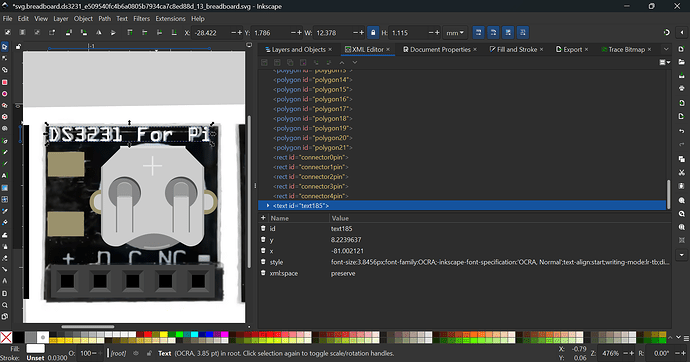
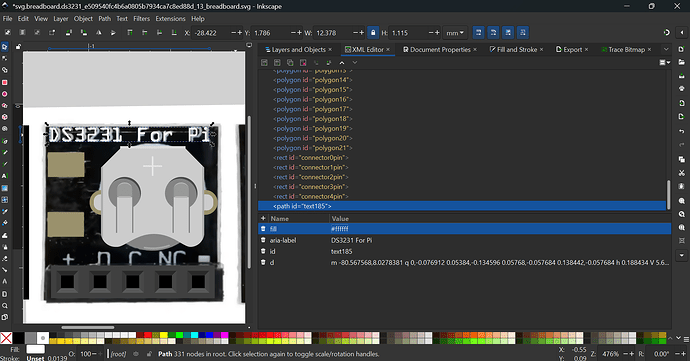
Add the text (in OCRA font, e.g.)
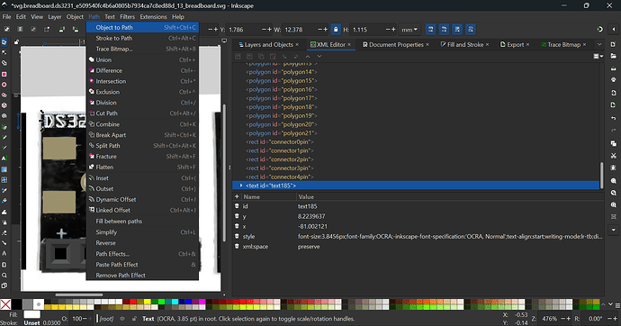
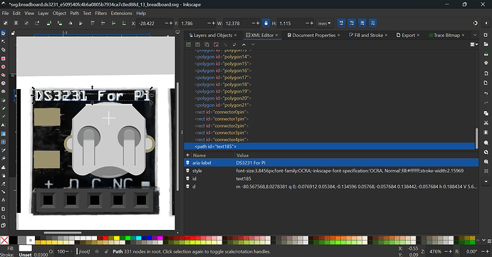
and convert to path
Delete the style attribute and replace with
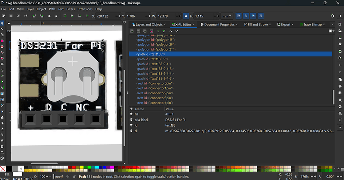
Repeat for all other texts.
Next, shift all the texts (now paths) to before the connectors
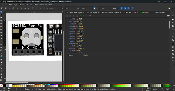
and put the rectangle back on the image
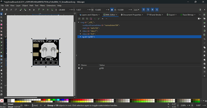
Delete the image, group everything
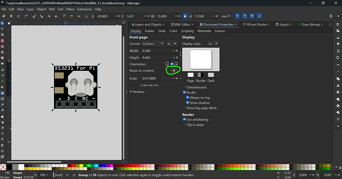
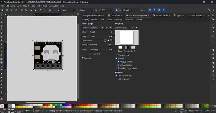
Then ctrl+shift+D or cmd+shift+D to go to document properties
and press the circled button. This resets the viewbox.
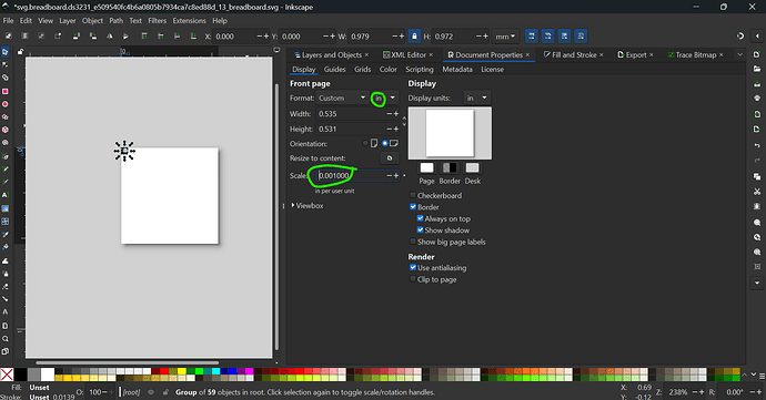
Now, change from
to
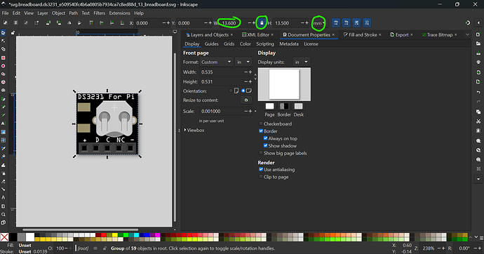
With height and width locked, change the width to 13.6
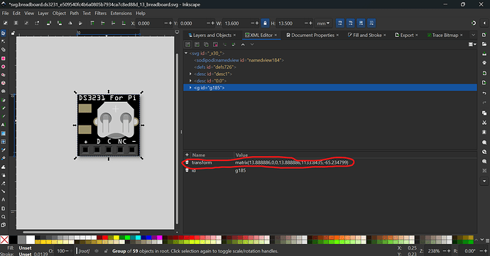
Now go to the XML Editor, and you’ll see something suspicious
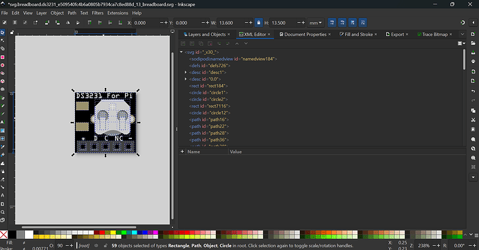
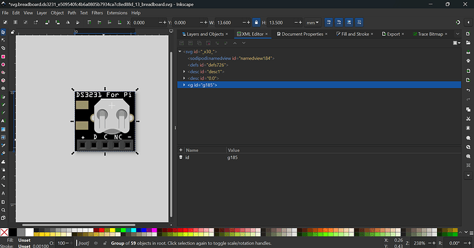
These numbers are the transforms of the group, which will be added after scaling and resetting of viewbox. To fix, ungroup
then regroup
NOTE: Do not SIMPLY DELETE THE TRANSFORMS
Instead, follow the above steps.
Next, change the group id to breadboard.
Now that you are done, save the file. Move on to schematic.
Model Answer
svg.breadboard.ds3231_e509540fc4b6a0805b7934ca7c8ed88d_13_breadboard (28 KB)
Schematic
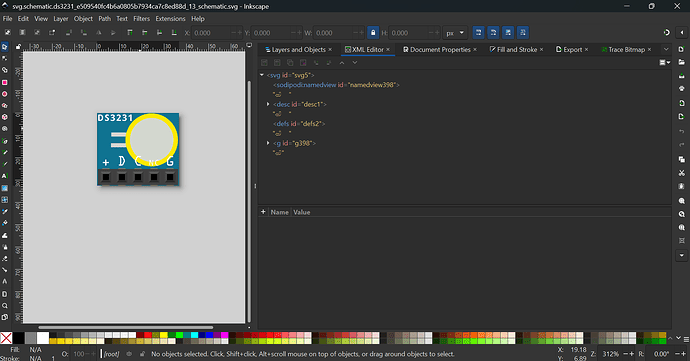
Now if you open the schematic, you will realise that the schematic layout is wrong.
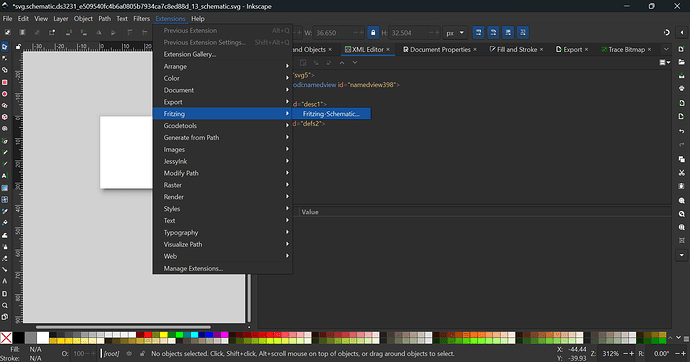
Delete all elements, and open the schematic extension
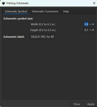
When prompted, set to
Note that the full text is
DS2131 RTC for RPi
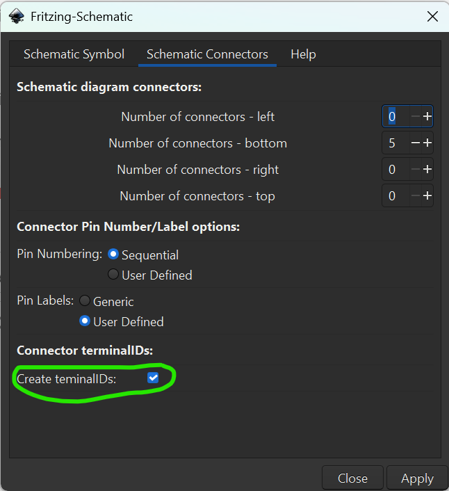
Next the connectors, set to
Remember to check the box.
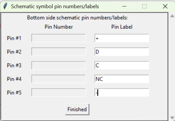
Next set the connectors
You can make the height smaller – your choice.
Model Answer
svg.schematic.ds3231_e509540fc4b6a0805b7934ca7c8ed88d_13_schematic (6 KB)
PCB
OK first start with the breadboard
To make sure that we won’t override the breadboard SVG, go to file → save as → double-click the PCB SVG file (at least on Windows)
You can also download this SVG (will be required in a while)
5-header_PCB (3 KB)
In the breadboard SVG, ungroup everything, and delete everything except for the headers
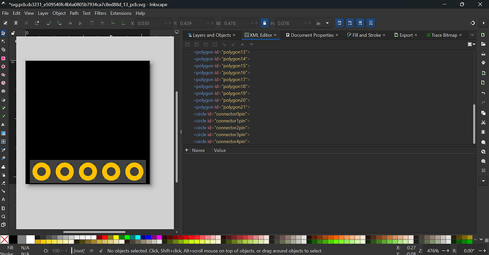
Delete all existing connectors, and grab the PCB connectors
Roughly estimate such that the connector is right in the middle of one pin header
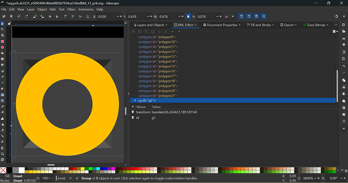
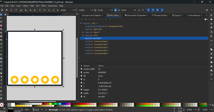
Then ungroup g1.
Now delete the headers
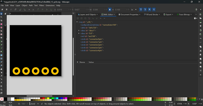
Now navigate to the rectangle, and change from
note: at this point please do not care about the copper groups
to
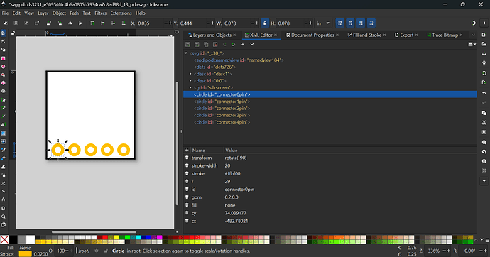
Group, reset the viewbox, ungroup
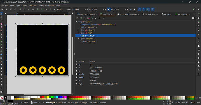
Now, group the rectangle and change the id to silkscreen
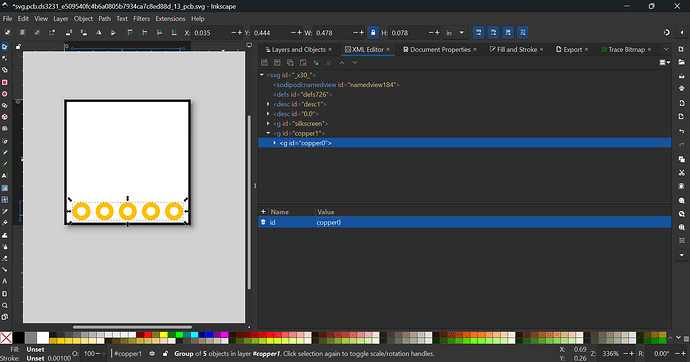
Next, group the remaining connectors twice
and change the id of the groups to
Save the file.
Model Ans
svg.pcb.ds3231_e509540fc4b6a0805b7934ca7c8ed88d_13_pcb
On to .fzp file
.fzp file
First, change from
<version>4</version>
<date>Do Mrz 7 2024</date>
<author>Florian Schäffer</author>
<description><!DOCTYPE HTML PUBLIC "-//W3C//DTD HTML 4.0//EN" "http://www.w3.org/TR/REC-html40/strict.dtd">
<html><head><meta name="qrichtext" content="1" /><style type="text/css">
p, li { white-space: pre-wrap; }
</style></head><body style=" font-family:'MS Shell Dlg 2'; font-size:8.25pt; font-weight:400; font-style:normal;">
<p style=" margin-top:0px; margin-bottom:0px; margin-left:0px; margin-right:0px; -qt-block-indent:0; text-indent:0px;">DS3231 with akku</p></body></html></description>
to
 <version>2</version>
 <date>Mon/Tue/Wed/Thu/Fri/Sat/Sun MMM DD YYYY</date>
 <author>Florian Schäffer, [your name]</author>
 <description></description>
Next, change from
<tags/>
to
 <tags>
  <tag>RPi</tag>
  <tag>Real Time Clock Module</tag>
  <tag>DS3231</tag>
 </tags>
For the properties, change from
 <properties>
  <property name="family">sensor</property>
  <property name="variant">variant 2</property>
 </properties>
to
 <properties>
  <property name="family">Real Time Clock Module</property>
  <property name="variant">DS3231</property>
  <property name="part number"/>
  <property name="layer"/>
  <property name="mn"/>
  <property name="mpn"/>
 </properties>
For views, change from
 <views>
  <breadboardView>
   <layers image="breadboard/ds3231_e509540fc4b6a0805b7934ca7c8ed88d_13_breadboard.svg">
    <layer layerId="breadboard"/>
   </layers>
  </breadboardView>
  <iconView>
   <layers image="icon/ds3231_e509540fc4b6a0805b7934ca7c8ed88d_13_icon.svg">
    <layer layerId="icon"/>
   </layers>
  </iconView>
  <schematicView>
   <layers image="schematic/ds3231_e509540fc4b6a0805b7934ca7c8ed88d_13_schematic.svg">
    <layer layerId="breadboard"/>
   </layers>
  </schematicView>
  <pcbView>
   <layers image="pcb/ds3231_e509540fc4b6a0805b7934ca7c8ed88d_13_pcb.svg">
    <layer layerId="breadboard"/>
   </layers>
  </pcbView>
 </views>
to
 <views>
  <breadboardView>
   <layers image="breadboard/ds3231_e509540fc4b6a0805b7934ca7c8ed88d_13_breadboard.svg">
    <layer layerId="breadboard"/>
   </layers>
  </breadboardView>
  <iconView>
   <layers image="breadboard/ds3231_e509540fc4b6a0805b7934ca7c8ed88d_13_breadboard.svg">
    <layer layerId="icon"/>
   </layers>
  </iconView>
  <schematicView>
   <layers image="schematic/ds3231_e509540fc4b6a0805b7934ca7c8ed88d_13_schematic.svg">
    <layer layerId="schematic"/>
   </layers>
  </schematicView>
  <pcbView>
   <layers image="pcb/ds3231_e509540fc4b6a0805b7934ca7c8ed88d_13_pcb.svg">
    <layer layerId="silkscreen"/>
    <layer layerId="copper1"/>
    <layer layerId="copper0"/>
   </layers>
  </pcbView>
 </views>
Now, the connectors (here are two example)
Change from
  <connector id="connector3" name="VCC" type="male">
   <description>VCC</description>
   <views>
    <breadboardView>
     <p svgId="connector3pin" layer="breadboard"/>
    </breadboardView>
    <schematicView>
     <p svgId="connector3pin" layer="breadboard"/>
    </schematicView>
    <pcbView>
     <p svgId="connector3pin" layer="breadboard"/>
    </pcbView>
   </views>
  </connector>
  <connector id="connector4" name="GND" type="male">
   <description>GND</description>
   <views>
    <breadboardView>
     <p svgId="connector4pin" layer="breadboard"/>
    </breadboardView>
    <schematicView>
     <p svgId="connector4pin" layer="breadboard"/>
    </schematicView>
    <pcbView>
     <p svgId="connector4pin" layer="breadboard"/>
    </pcbView>
   </views>
  </connector>
to
  <connector id="connector0" name="+" type="female">
   <description>pin1</description>
   <views>
    <breadboardView>
     <p svgId="connector0pin" layer="breadboard"/>
    </breadboardView>
    <schematicView>
     <p svgId="connector0pin" layer="schematic" terminalId="connector0terminal"/>
    </schematicView>
    <pcbView>
     <p svgId="connector0pin" layer="copper1"/>
     <p svgId="connector0pin" layer="copper0"/>
    </pcbView>
   </views>
  </connector>
  <connector id="connector1" name="D" type="female">
   <description>pin2</description>
   <views>
    <breadboardView>
     <p svgId="connector1pin" layer="breadboard"/>
    </breadboardView>
    <schematicView>
     <p svgId="connector1pin" layer="schematic" terminalId="connector1terminal"/>
    </schematicView>
    <pcbView>
     <p svgId="connector1pin" layer="copper1"/>
     <p svgId="connector1pin" layer="copper0"/>
    </pcbView>
   </views>
  </connector>
Do the similar for the other 3
Need help?
change from
  <connector id="connector5" name="SCL" type="male">
   <description>SCL</description>
   <views>
    <breadboardView>
     <p svgId="connector5pin" terminalId="connector5terminal" layer="breadboard"/>
    </breadboardView>
    <schematicView>
     <p svgId="connector5pin" terminalId="connector5terminal" layer="breadboard"/>
    </schematicView>
    <pcbView>
     <p svgId="connector5pin" terminalId="connector5terminal" layer="breadboard"/>
    </pcbView>
   </views>
  </connector>
  <connector id="connector6" name="SDA" type="male">
   <description>SDA</description>
   <views>
    <breadboardView>
     <p svgId="connector6pin" layer="breadboard"/>
    </breadboardView>
    <schematicView>
     <p svgId="connector6pin" layer="breadboard"/>
    </schematicView>
    <pcbView>
     <p svgId="connector6pin" layer="breadboard"/>
    </pcbView>
   </views>
  </connector>
to
  <connector id="connector2" name="C" type="female">
   <description>pin3</description>
   <views>
    <breadboardView>
     <p svgId="connector2pin" layer="breadboard"/>
    </breadboardView>
    <schematicView>
     <p svgId="connector2pin" layer="schematic" terminalId="connector2terminal"/>
    </schematicView>
    <pcbView>
     <p svgId="connector2pin" layer="copper1"/>
     <p svgId="connector2pin" layer="copper0"/>
    </pcbView>
   </views>
  </connector>
  <connector id="connector3" name="NC" type="female">
   <description>pin4</description>
   <views>
    <breadboardView>
     <p svgId="connector3pin" layer="breadboard"/>
    </breadboardView>
    <schematicView>
     <p svgId="connector3pin" layer="schematic" terminalId="connector3terminal"/>
    </schematicView>
    <pcbView>
     <p svgId="connector3pin" layer="copper1"/>
     <p svgId="connector3pin" layer="copper0"/>
    </pcbView>
   </views>
  </connector>
    <connector id="connector4" name="-" type="female">
   <description>pin5</description>
   <views>
    <breadboardView>
     <p svgId="connector4pin" layer="breadboard"/>
    </breadboardView>
    <schematicView>
     <p svgId="connector4pin" layer="schematic" terminalId="connector4terminal"/>
    </schematicView>
    <pcbView>
     <p svgId="connector4pin" layer="copper1"/>
     <p svgId="connector4pin" layer="copper0"/>
    </pcbView>
   </views>
  </connector>
Get rid of the <buses/> tag as we don;t need it.
Instead, change the <url/> tag to
<url>https://www.aliexpress.com/i/32918840010.html</url>
Save the file
Icon
Delete the file as not needed
Putting everything together
Finally, zip the file into a .fzpz file and check for any errors. Good luck!
Here is the fixed part that you should get
RTC DS3231-fixed.fzpz (10.3 KB)
