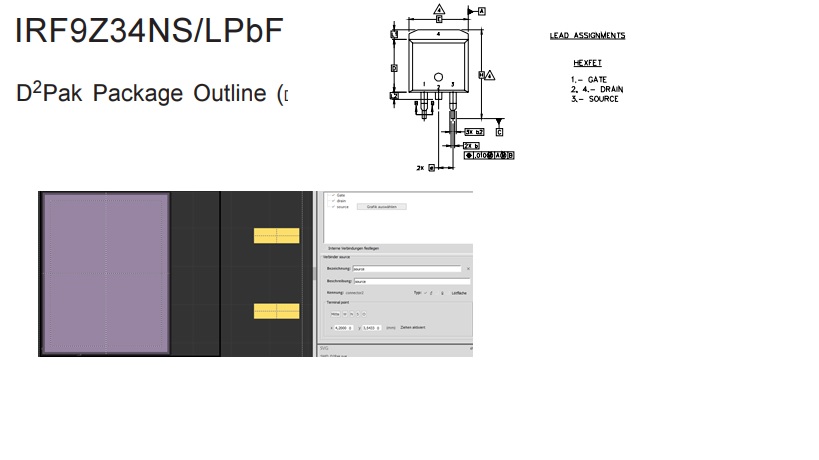
At the part p-Channel MosFET layout D2Pak the source and drain are mixed up, the smaller DPAK is ok. Because of current problems I changed in my circuit from TSM680P06CP (DPAK) to IRF9Z34NSPBF (D2PAK) and noticed that in DPAK source and drain are in the right order and in D2PAK source and drain are mixed up
Version 0.9.7
(bCD-534-0-120da230 2021-07-12) 64 [Qt 5.15.2]
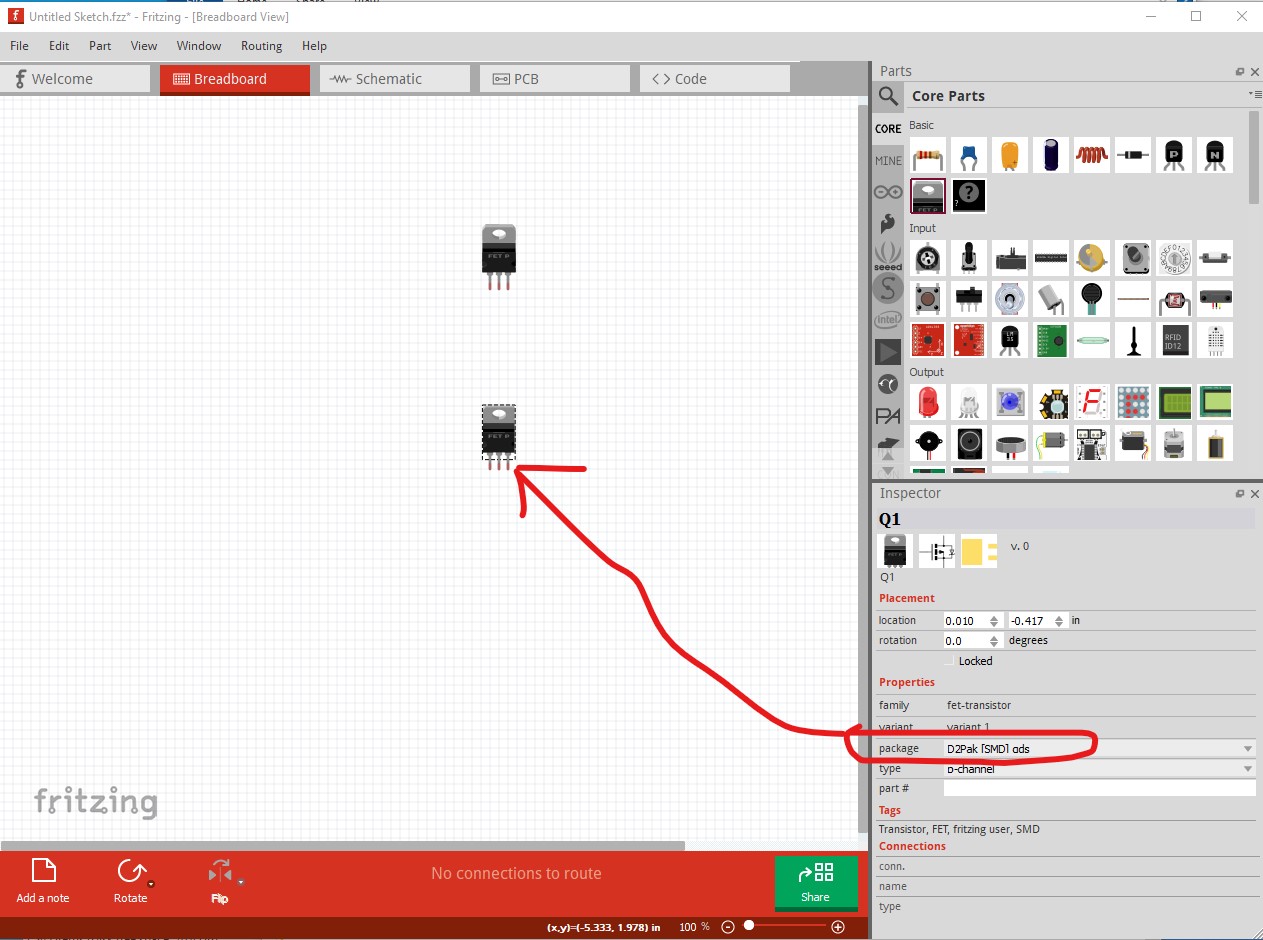
Yep, that is one of the most screwed up parts I have seen in core parts. It has many problems, as you have no doubt discovered if you have tried to fix it (dimensions in px, which screws up the scale, unwanted rx and ry in the pcb rectangles which turn them in to circles, incorrect scales, etc.) Here is a corrected part that I think will do the job. Note before ordering boards print out the pcb footprint at 1:1 scale and compare it to a real part to make sure the footprint is correct as the data sheet wasn’t entirely clear.