Hello,
I want to create my own PCB shape.
How can I do that with fritzing?
I am only finding fixed shaped PCB’s and no tool which allows me to reshape a rectangle PCB (for example).
My best regards, Matthias
You need to create an svg file with the custom shape in inkscape or some other graphics editor. Here are some instructions
I don’t know why you have been working on this for a few days… It only takes a few minutes to make one… Just kidding…
See attached, This is a Donut I made for andy, http://imgh.us/Andys_Donut.svg , to see how it is written.
You need the layer: “board” with the object “boardoutline”. this needs to be a single object.
Layer: “silkscreen” is the top of the board and the Layer: “silkscreen0” is the bottom, Silkscreens can have as many objects as you would like.
<g id="board"> <path id="boardoutl…
The overview given at http://fritzing.org/pcb-custom-shape/ is a good start, but I believe it’s a little outdated and missing a couple of important details.
The instructions on that page say at the bottom to set the ID to “board” and “silkscreen” in Object properties or the XML Editor, However, it’s the layer that needs those IDs, not the Objects. I usually set the Object ID to something related for clarity, but it’s not even necessary.
[image]
You can do a search of Fritzing and find more post.
Hi, yes, this is working up to the point where you want to produce that board. This is the message the fritzing PCB service states on upload of my board:
I already added a layer “dimension” tp the svg and it has the same info as the “silkscreen”.
Fritzing is using a new service (aisler.net ).
Do you have any idea what to do now?
My best regards,
Matthias
Here is the solution for that:
Hello,
I want to produce a custom shaped PCB by aisler.net (former fritzing.fab). I did this for createing the PCB:
http://fritzing.org/pcb-custom-shape/
frintzing can handle the custom shaped board.
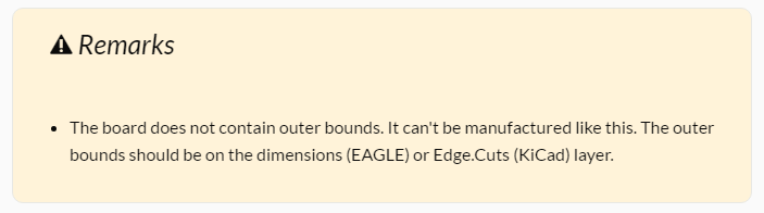
But on uploading to aisler.net , I get this error message:
[image]
I already added a “dimensions” layer to my svg. It has the same content as the “silkscreen” layer.
But the error message remains.
Can anybody help here?
My best regards,
Matthias
Yes, it is possible to design your PCB in any shape and size. You can design your PCB shape according to you. There are a number of tools that used to make the PCB shapes.