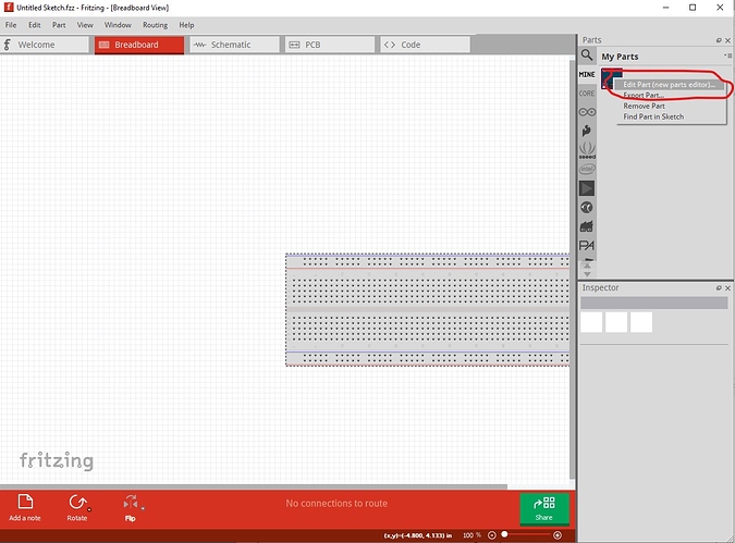
OK here are two ways to do it. Load the current part in to Fritzing, select the part in the mine parts bin and right click and select Edit Part (new parts editor)
Then click File->show in folder which produces this
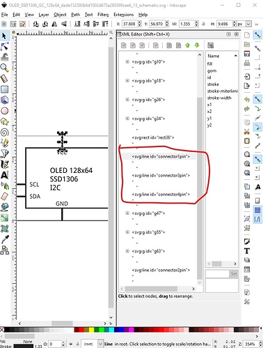
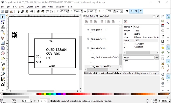
click on the svg file to load it in to Inkscape
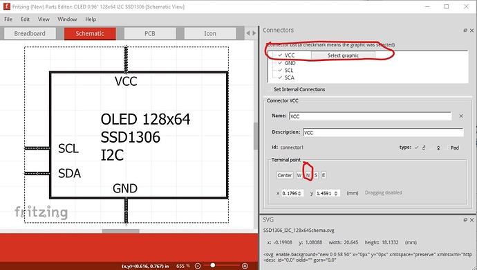
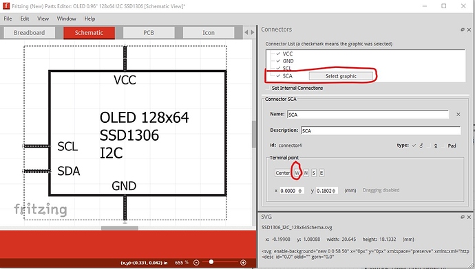
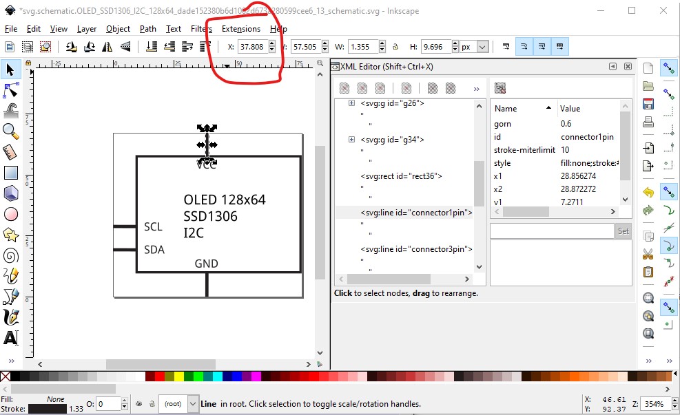
where we see the connectors (1 to 3) pins but no connectorxterminals. Now back to parts editor and click on VCC (circled in red in the image) and then on Select graphic. Then click on N in the Terminal point window below to set the terminalId at the top of the VCC pin (North)
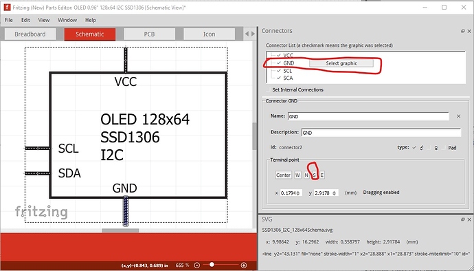
repeat for GND and select S (south) to set the terminal at the bottom of the gnd pin.
Now do the same on SCL selecting W (to set the terminal on the left of the SCL pin)
and last repeat the above for SCA
Now click File->save and OK to the prompt that comes up to save the changes to the part.
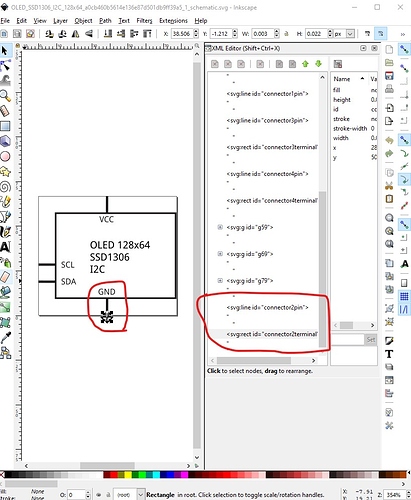
and load the latest one in Inkscape
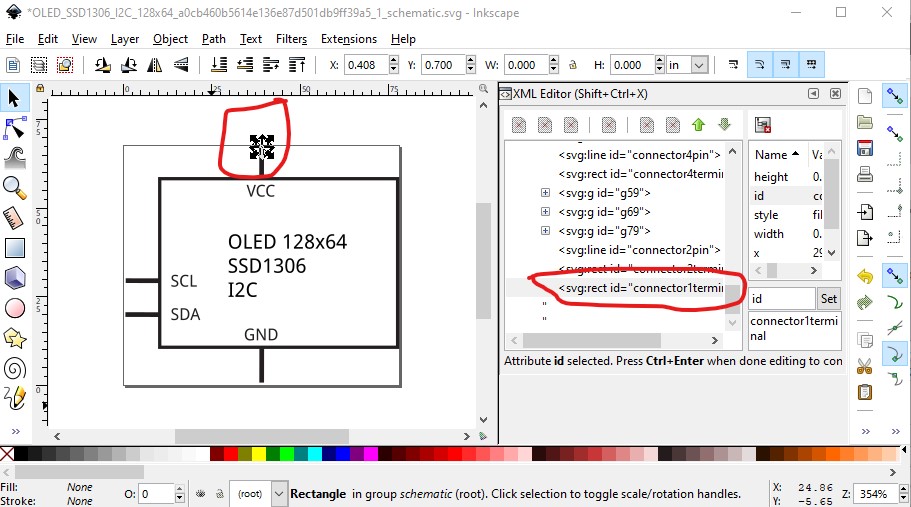
where we see that connector2 now has a new entry called connector2terminal which is a square positioned at the bottom of the pin as we requested. We also see that the terminal on connector1 is missing (which is one reason I dislike using parts editor!) so we would need to go back and do that one again until it appears.
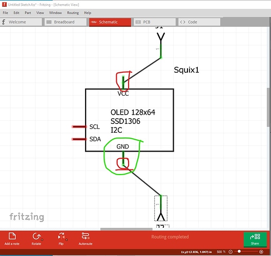
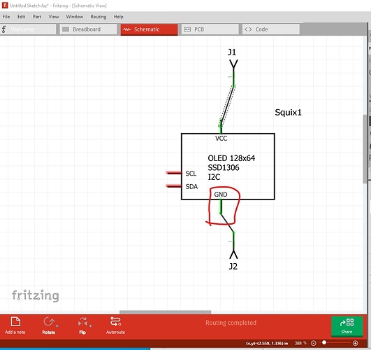
When I now drag the edited part in to the sketch in schematic and connect 1 pin headers to both VCC and GND we see the results (and an error!)
Here we see VCC still connects to the center of the pin (because it has no terminalId) but GND on the bottom connects to the end of the pin as it should. However because the pin has line-cap set to butt instead of rounded there is a small gap between the wire and the pin which is incorrect, and the end of the pin does not align with the .1in grid lines. To fix these two errors we need to edit the svg file.
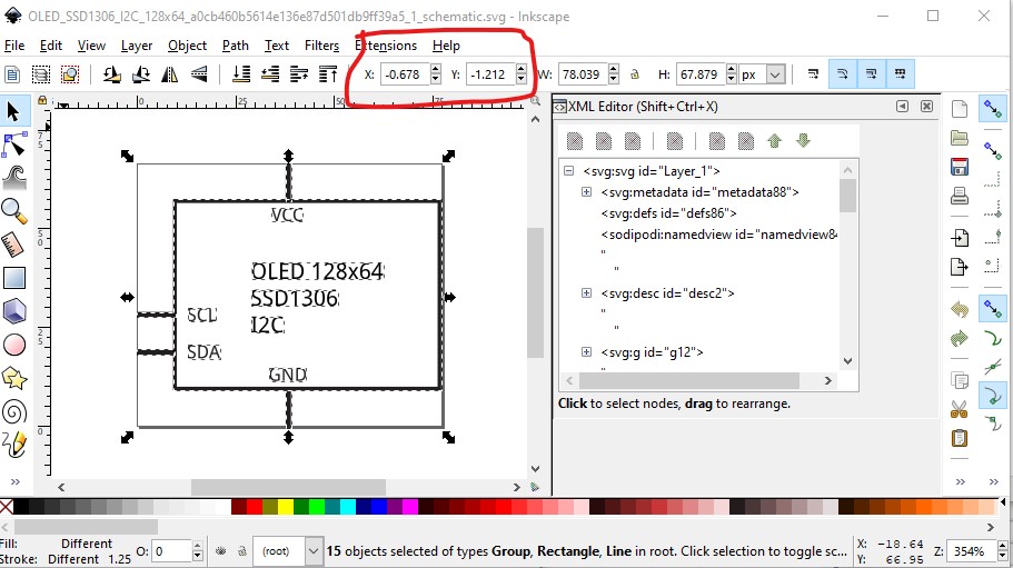
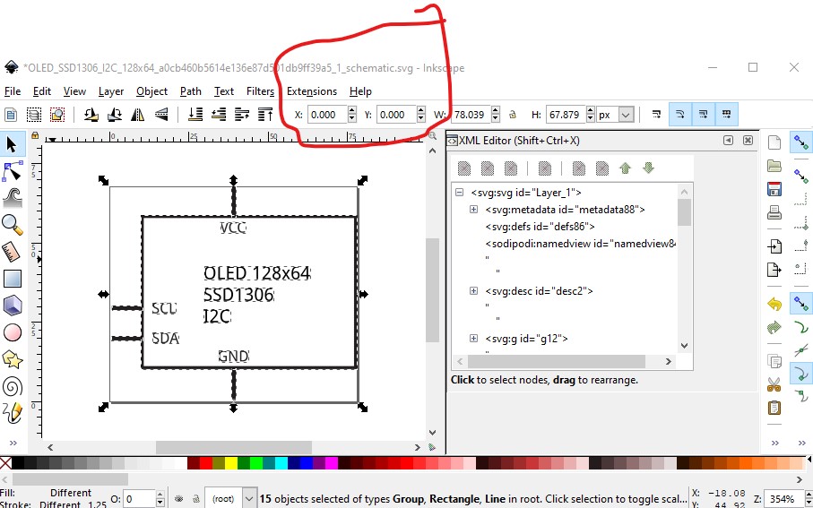
Here we see that the view box is not starting at 0 0 as Fritzing expects. This is the cause of the offset in Y on the pins. To correct this click Edit->select all to select the entire drawing, then Edit->resize page to selection to reset the view box to 0 which produces this
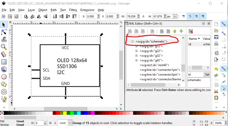
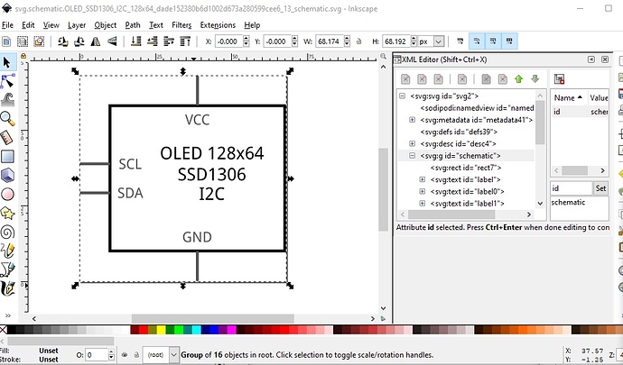
Now with the entire drawing selected click Object->group to create a group of the entire document and name the group schematic like this
Then I duplicated connector2terminal, named the new rectange connector1terminal and moved it .8in up in Y to be at the top of connector1pin.
Now on each pin I changed the style attribute to add a stroke-linecap:round to change the end ot the pin from flat to having a dome so the wire will connect correctly. Then I did an Edit->select all and Edit->Resize page to selection to reset the viewbox to include the entire document (you should always do this at the end of an edit session!) Then I save as plain svg. Now if I reload the part things should work correctly, but they don’t because I was lazy and didn’t ungroup.
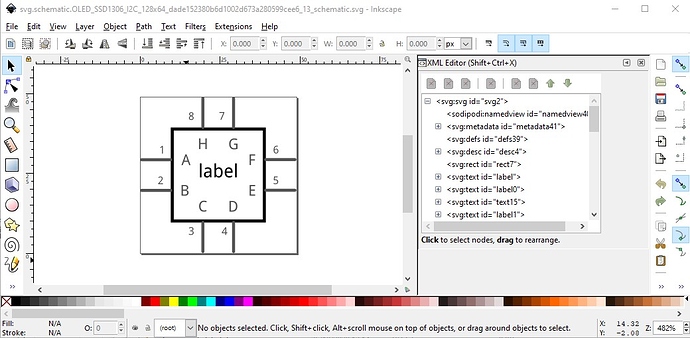
The lines have round end caps, but the pins are offset slightly (the red is the pin and it is not on top of the line as it should be) and the pins are still not aligned to the grid. There appears to be something unknown wrong in this svg. Rather than try and figure out what it is, I choose to use the schematic template from here
and make a new svg like this.
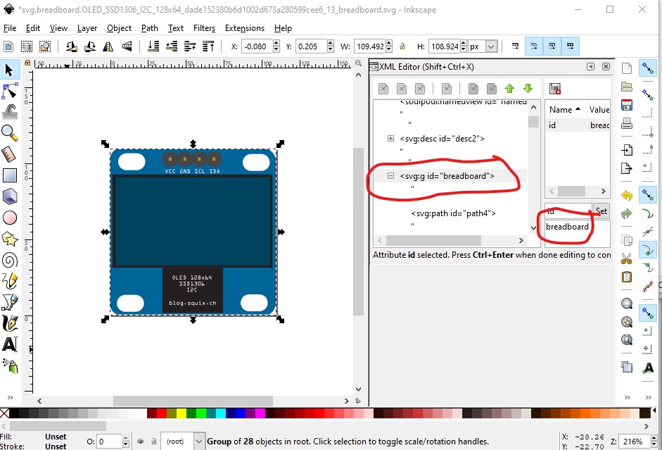
Then I editted the breadboard svg and renamed group g104 to breadboard to create a layerId and saved as plain svg.
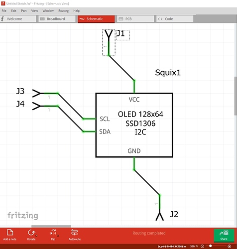
then rebuilt the fzpz file which now works. In schematic the pins align to the grid, and the wires connect (without gaps) to the end of the pins as they should
This came from this new part
OLED_096_128x64_I2C_SSD1306.fzpz (7.3 KB)
Peter
