Over all not a bad job, but a few problems ( illustrated via extra.fzz below):
Breadboard:
Capacitive moisture sensor: you may want to add a connectorxterminal definition to the connector in the breadboard svg and move it to the edge of the connector so the wires terminate on the edge of the board instead of the middle of the pin as they do now although it is OK as it is now too. Otherwise breadboard looks fine.
Schematic:
Most of the parts are either lacking a connectorxterminal definition or it is incorrect (such as being a group rather than a rectangle). That is what is causing the lines connecting at an angle to connect in the middle of the pin instead of the outside edge as they should. If you canāt figure out how to correct this, post and Iāll look at the svgs and post the solution. The soil moisture sensor has correct terminals (the lines terminate at the edge as they should) but the āAā pin should be moved so it aligns with the .1 in grid for better readablility. The DS18B20 pins need to be moved a bit so that they align with the .1 grid, the out pin has a correct terminal definition but the power pins donāt appear to. Iām not sure why there are extra rats nest lines on the nodeCPU ground that may have been a problem on my part somehow (it usually indicates corruption in the parts database file due to Fritzing bugs) and they all appear to lack terminal definitions.
PCB looks fine (I didnāt export the gerbers and check drill hole sizes but presumably they are correct).
thanks a lot for your feedback. These are my first parts. Iāll try to fix the connectors as fast as possible. I didnāt check my parts in that way, but Iāll Keep that in mind for new parts.
Good job for first parts, not many and not serious errors. I find that particular test (groups or single connectors connecting to all the pins) finds most of the common errors in parts and makes sure the connections are consistent across all three views. If you have problems feel free to ask, always happy to help people make parts (its what Fritzing needs to thrive ).
As well as defining the terminalid in the svg. With only the svgid definition the terminal defaults to the middle of the shape defined as the pin which isnāt what we want in this case. Here is a copy of the part with the fpz modified to add the terminal id, and the svg modified to move the terminal definition to the edge of the pin:
Hi Peter, with the current PCB layout, the parts are facing the backside of the NodeMCU board. I prefer the parts facing the outside, necessitating the mirror image of the PCB board. Currently, I have manually moved the wiring to the opposite row of connections in order to accomplish this, which is cumbersome. Is it possible to create a mirror image of the PCB board. In other words, flip horizontally!
Rgds
Dick
Luckily I resisted the temptation to say this will be done in about 15 minutes, because while your requested change is trivial and only took 15 minutes, when I tested it I discovered that the base isnāt one of those that I fixed up (when I thought it was) and has a number of errors. So here are two new files which fix up the visible errors (the internals are still a mess and need a major cleaning ). The NodeMCUv3 Lolin_1.1_inch_rev_pcb.fzpz file is your requested swap of the pcb in horizontal (with the addition of a square on pin 1 on the pcb copper and a note the it is rev pcb on the schematic to tell them apart) and NodeMCUv3 Lolin_1.1_inch_fixed_schem.fzpz is the original part with the fixes applied to it (and should replace the original part). At some point Iāll clean the rest of it up and feed it back to the original author.
@vanepp, I know it has been a while, but I read your post where you made a fzpz file with 1.1 inch spacing between the rows. When I downloaded it, It is still no bigger than the .9 inch one I have on my MB102 breadboard view or the PCB view. But when I print out the svg and print at 100% it is the right size. I donāt understand. I did have to modify the part file āmoduleIdā because when I tried to import it, Fritzing said I already had a part with that name.
I have run into this when downloading parts Vanepp has made. My solution was to look in the fritzing parts folder and delete the original with the matching moduleid and then import his new part.
@sublimeartistry I appreciate the quick reply. Under different circumstances, I would use your suggestion. However, the NodeMCU board is open source and some have the pin rows .9 inch apart and some 1.1 inch apart. I would like to have both in my parts bin, not one or the other.
I think the one I posted is probably a copy of the original on github (which in turn may be created from an existing part in core). If so this one (which is the one I posted, edited with parts editor but not changed, and exported as a new part) should do what you want without conflicting with any existing part as it has a new moduleid.
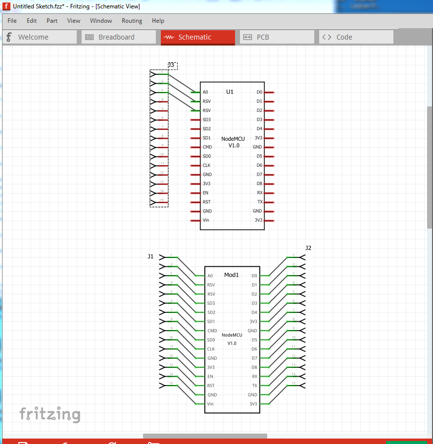
Indeed they are in addition to number of other problems. For hole sizes, assuming Inkscape (I think the others. at least Corel Draw, are different), hole size is calculated by hole size = Diameter of pad - (2 * stroke-width) . So to get a .038in hole suitable for a .1 header pin, and assuming a standard 20 thou stroke-width and standard scale (none of which are true in the original ), the calculation is pad diameter = 0.078in, stroke-width 20, so 78 - 40 = 38 (in thou) or 0.038in for the hole. This will work at any scale, the math is just more difficult at incorrect scales. The other major problem in the original is the lack of schematic terminalIds which causes the connection to the middle of the pin like this )the top one is the original part without terminalIds)
Also the pins are out of sequence (they jump at around pin 20 to the 32 range) and the scale of the svgs are all incorrect. I fixed all of that up in this new part, which is ready to submit to core parts when someone gets around to doing so: